-
TPSM82902, 2-A, 3-V to 17-V, High Efficiency and Low IQ Buck Converter Module in a MicroSiPTM Package with an Integrated Inductor
- 1 Features
- 2 Applications
- 3 Description
- 4 Revision History
- 5 Pin Configuration and Functions
- 6 Specifications
-
7 Detailed Description
- 7.1 Overview
- 7.2 Functional Block Diagram
- 7.3
Feature Description
- 7.3.1 Mode Selection and Device Configuration (MODE/S-CONF)
- 7.3.2 Adjustable VO Operation (External Voltage Divider)
- 7.3.3 Setable VO Operation (VSET and Internal Voltage Divider)
- 7.3.4 Soft Start/Tracking (SS/TR)
- 7.3.5 Smart Enable with Precise Threshold
- 7.3.6 Power Good (PG)
- 7.3.7 Undervoltage Lockout (UVLO)
- 7.3.8 Current Limit And Short Circuit Protection
- 7.3.9 Thermal Shutdown
- 7.4 Device Functional Modes
- 8 Application and Implementation
- 9 Device and Documentation Support
- 10Mechanical, Packaging, and Orderable Information
- IMPORTANT NOTICE
Package Options
Mechanical Data (Package|Pins)
- SIS|11
Thermal pad, mechanical data (Package|Pins)
Orderable Information
TPSM82902, 2-A, 3-V to 17-V, High Efficiency and Low IQ Buck Converter Module in a MicroSiPTM Package with an Integrated Inductor
1 Features
- High efficiency for wide duty cycle and load range
- IQ: 4-µA typical
- 62-mΩ high-side and 22-mΩ low-side RDS(ON)
- 3-mm × 2.8-mm × 1.6-mm MicroSiP™ package
- Up to 2-A continuous output current
- ±0.9%
feedback voltage accuracy across temp
(–40°C to 125°C) - Configurable output voltage options:
- VFB external divider: 0.6 V to 5.5 V
- VSET internal divider: 16 options between 0.4 V and 5.5 V
- DCS-Control topology with 100% mode
- Flexibility through MODE/S-CONF pin
- 2.5-MHz or 1.0-MHz switching frequency
- Forced PWM or auto (PFM) power save mode with dynamic mode change option
- Automatic efficiency enhancement (AEE)
- Output discharge on/off
- Highly flexible and easy to use
- Optimized pinout for single-layer routing
- Precise enable input
- Power-good output
- Adjustable soft start and tracking
- No external bootstrap capacitor required
- Create a custom design using the TPSM82902 using the WEBENCH® Power Designer
3 Description
The TPSM82902 is a highly efficient, small, and flexible synchronous step-down DC-DC converter MicroSiP package module that is easy to use. A selectable switching frequency of 2.5 MHz or 1.0 MHz allows the use of small components and provides fast transient response. The device supports high VOUT accuracy of ± 1% with the DCS-Control topology. The wide input voltage range of 3 V to 17 V supports a variety of nominal inputs, like 12-V supply rails, single-cell or multi-cell Li-Ion, and 5-V or 3.3-V rails.
The TPSM82902 can automatically enter power save mode (if auto PFM/PWM is selected) at light loads to maintain high efficiency. Additionally, to provide high efficiency at very small loads, the device has a low typical quiescent current of 4 µA. AEE, if enabled, provides high efficiency across VIN, VOUT, and load current. The device includes a MODE/Smart-CONF input to set the internal/external divider, switching frequency, output voltage discharge, and automatic power save mode or forced PWM operation.
The device is available in small 11-pin MicroSiP package measuring 3.0 mm × 2.8 mm × 1.6 mm with an integrated 1-μH inductor.
| PART NUMBER | PACKAGE(1) | BODY SIZE (NOM) |
|---|---|---|
| TPSM82902 | SIS (uSiP, 11) | 3.00 mm × 2.80 mm |
 Simplified Schematic
Efficiency Versus Output Current (1.2 VO at 2.5 MHz, Auto PFM/PWM)
4 Revision History
| DATE | REVISION | NOTES |
|---|---|---|
| November 2022 | * | Initial Release |
5 Pin Configuration and Functions

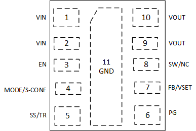
Figure 5-1 11-Pin SIS MicroSiP™ Package (Top View, Device Pins Face Down)
| Pin | I/O | Description | |
|---|---|---|---|
| Name | Number | ||
| VIN | 1, 2 | I | Power supply input pin. Ensure the input capacitor is connected as close as possible between the VIN and GND pins. |
| EN | 3 | I | Enable input pin. Connect to logic low to disable the device. Pull high to enable the device. Do not leave this pin unconnected. |
| MODE/ S-CONF | 4 | I | Device mode selection (auto PFM/PWM or forced PWM operation) and SmartConfig™ application. Connect high, low, or to a resistor to configure the device according to Table 7-2. Do not leave this pin unconnected. |
| SS/TR | 5 | I | Soft start/tracking pin. An external capacitor connected from this pin to GND defines the rise time for the internal reference voltage. The pin can also be used as an input for tracking and sequencing. The pin can be left floating for the fastest ramp-up time. |
| PG | 6 | O | Open-drain power-good output. High = VOUT is ready. Low = VOUT is below nominal regulation. This pin requires a pullup resistor. |
| FB/VSET | 7 | I | Depends on device configuration (see Section 7.3.1)
|
| SW/NC | 8 | NC | Switch pin of the converter. Do not connect, leave floating. |
| VOUT | 9, 10 | O | Output voltage pin. Connect directly to the positive pin of the output capacitor. |
| GND | 11 | — | Ground pin. It must be connected directly to the common ground plane. It must be soldered to achieve appropriate power dissipation and mechanical reliability. |