SLVSGJ4C October 2022 – July 2023 TPSM82912 , TPSM82913 , TPSM82913E
PRODUCTION DATA
- 1
- 1 Features
- 2 Applications
- 3 Description
- 4 Revision History
- 5 Pin Configuration and Functions
- 6 Specifications
-
7 Detailed Description
- 7.1 Overview
- 7.2 Functional Block Diagram
- 7.3
Feature Description
- 7.3.1 Smart Config (S-CONF)
- 7.3.2 Device Enable (EN/SYNC)
- 7.3.3 Device Synchronization (EN/SYNC)
- 7.3.4 Spread Spectrum Modulation
- 7.3.5 Output Discharge
- 7.3.6 Undervoltage Lockout (UVLO)
- 7.3.7 Power-Good Output
- 7.3.8 Noise Reduction and Soft-Start Capacitor (NR/SS)
- 7.3.9 Current Limit and Short-Circuit Protection
- 7.3.10 Thermal Shutdown
- 7.4 Device Functional Modes
- 8 Application and Implementation
- 9 Device and Documentation Support
- 10Mechanical, Packaging, and Orderable Information
Package Options
Mechanical Data (Package|Pins)
- RDU|28
Thermal pad, mechanical data (Package|Pins)
Orderable Information
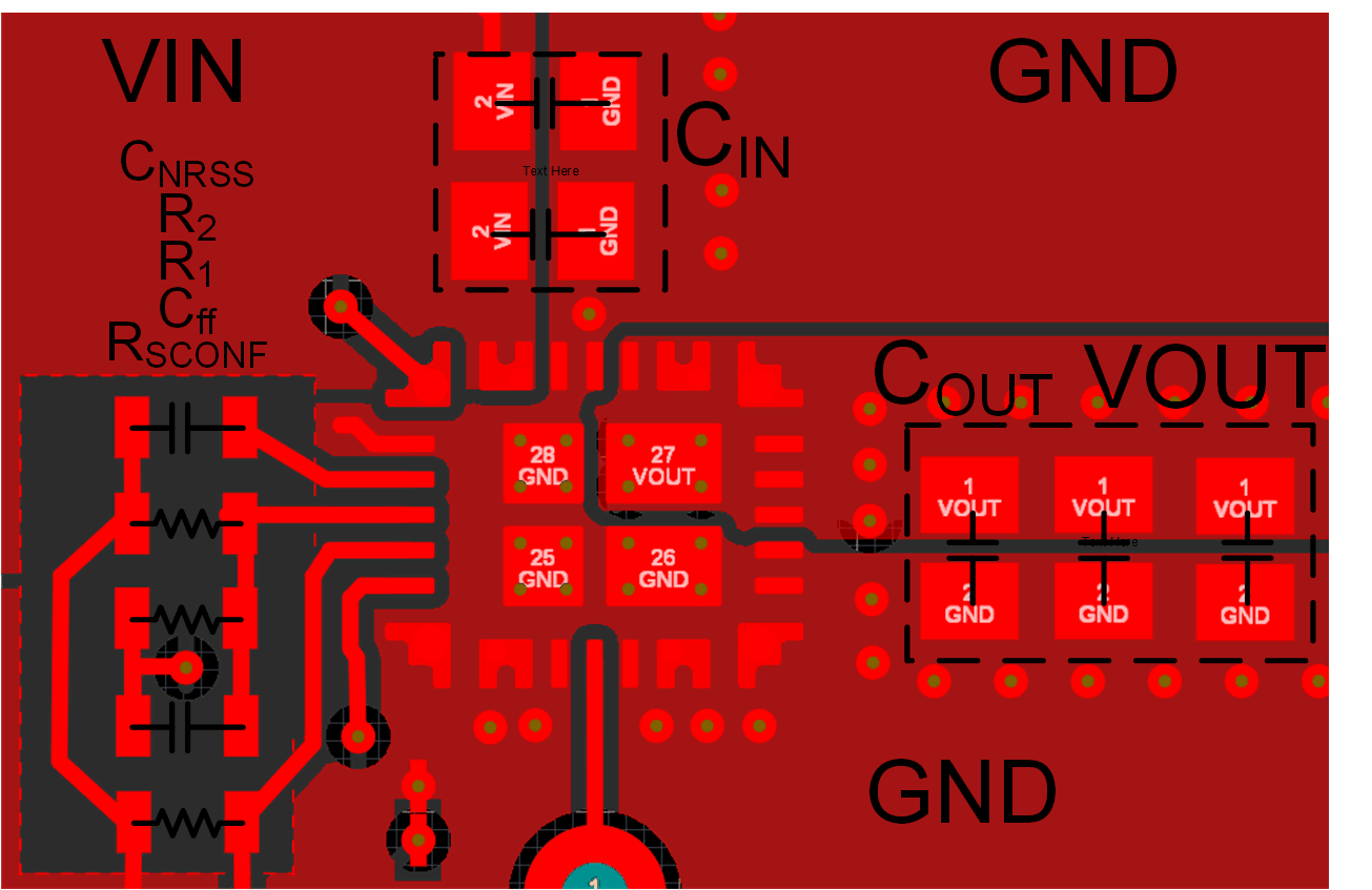
8.4.2 Layout Example
 Figure 8-15 Recommended
Layout for Single L-C Filter
Figure 8-15 Recommended
Layout for Single L-C FilterNote: For a single L-C configuration, the feedback
sense is placed near the VOUT capacitors. For a second L-C filter
design, the feedback sense is placed near the load after the
VOUT_FILT capacitors.
 Figure 8-16 Recommended
Layout for Design with Second L-C Filter
Figure 8-16 Recommended
Layout for Design with Second L-C FilterNote: The ferrite bead can be placed closer to the
device as long as it is placed > 8 mm from the device. This
placement avoids capacitive and electromagnetic coupling to the
output of the ferrite bead. If the ferrite bead is placed < 8 mm,
the filtering effect of the ferrite bead is greatly reduced. If the
ferrite bead is routed through a via to the back side of the board,
ensure adequate ground plane between the layers if the ferrite bead
is in this area.