VIN = 12 V, VOUT = 1.2 V, TA = 25°C, BOM = Table 8-1, (unless
otherwise noted)

| |
|
|
| 12 V to 1.2 V, 1 A |
2.2 μH, 1 MHz |
First L-C Only |
Figure 6-1 VOUT Ripple After the First L-C Filter 
| |
|
|
| 12 V to 1.2 V, 1 A |
2.2 μH, 1
MHz |
First and second
L-C |
Figure 6-3 VOUT Ripple After the Second L-C Filter
| 12 V to 1.8 V, 1 A |
2.2 μH, 1 MHz |
First L-C Only |
| |
|
|
Figure 6-5 VOUT Ripple After the First L-C Filter 
| 12 V to 1.8 V, 1 A |
2.2 μH, 1 MHz |
First and second
L-C |
| |
|
|
Figure 6-7 VOUT Ripple After the Second L-C Filter
| 12 V to 3.3 V, 1 A |
2.2 μH, 2.2 MHz |
First L-C Only |
| |
|
|
Figure 6-9 VOUT Ripple After the First L-C Filter 
| 12 V to 3.3 V, 1 A |
2.2 μH, 2.2 MHz |
First and second
L-C |
|
|
|
Figure 6-11 VOUT Ripple After
the Second L-C Filter
| 5 V to 1.2 V, 1 A |
2.2 μH, 2.2 MHz |
First L-C Only |
| |
|
|
Figure 6-13 VOUT Ripple After the First L-C Filter 
| 5 V to 1.2 V, 1 A |
2.2 μH, 2.2 MHz |
First and second
L-C |
| |
|
|
Figure 6-15 VOUT Ripple after the Second L-C Filter
| 5 V to 1.8 V, 1 A |
2.2 μH, 2.2 MHz |
First L-C Only |
| |
|
|
Figure 6-17 VOUT Ripple After the First L-C Filter 
| 5 V to 1.8 V, 1 A |
2.2 μH, 2.2 MHz |
First and second
L-C |
| |
|
|
Figure 6-19 VOUT Ripple After the Second L-C Filter
| 5 V to 3.3 V, 1 A |
2.2 μH, 2.2 MHz |
First L-C Only |
| |
|
|
Figure 6-21 VOUT Ripple After the First L-C Filter 
| 5 V to 3.3 V, 1 A |
2.2 μH, 2.2 MHz |
First and second
L-C |
| |
|
|
Figure 6-23 VOUT Ripple After the Second L-C Filter
| 6 V to 1.2 V, 1 A |
2.2 μH, 1 MHz |
BW = 50 Hz |
| S-CONF = OFF,
Triangular, Random |
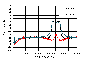
Figure 6-25 Spread Spectrum FFT - 50-Hz BW
| 12 V to 1.2 V |
1 MHz |
After ferrite bead
filter |
| NR/SS = Open, 220 nF, 470 nF, 2.2 μF, BW = 100 Hz to
100 kHz |
Figure 6-27 Output Noise Density vs Frequency
| 12 V to 3.3 V |
2.2 MHz |
After ferrite bead
filter |
| NR/SS = Open, 220 nF, 470 nF, 2.2 μF, BW = 100 Hz to
100 kHz |
Figure 6-29 Output Noise Density vs Frequency
| 5 V to 1.8 V |
2.2 MHz |
After ferrite bead
filter |
| NR/SS = Open, 220 nF, 470 nF, 2.2 μF, BW = 100 Hz to
100 kHz |
Figure 6-31 Output Noise Density vs Frequency
| 12 V to 1.2 V |
2.2 μH, 1 MHz |
1 A, 2 A, 3 A |
| After ferrite bead filter |
Figure 6-33 PSRR
vs Frequency
| 12 V to 3.3 V |
2.2 μH, 2.2 MHz |
1 A, 2 A, 3 A |
|
After ferrite bead
filter |
|
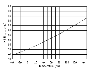
Figure 6-35 PSRR vs Frequency Figure 6-37 Low-Side RDS(ON) vs Junction Temperature
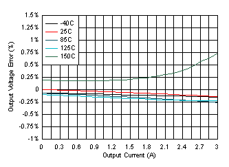
 Figure 6-39 Output Voltage Error vs Load
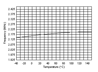
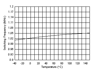
 Figure 6-41 Oscillator Frequency vs Temperature
 Figure 6-43 Output Discharge Resistance vs Output Voltage
|
BW = 10
kHz |
|
| 12 V to 1.2 V, 1 A |
2.2 μH, 1
MHz |
First L-C Only |
Figure 6-2 VOUT Ripple FFT After the First L-C Filter 
|
BW = 10 kHz |
|
| 12 V to 1.2 V, 1 A |
2.2 μH, 1
MHz |
First and second
L-C |
Figure 6-4 VOUT Ripple FFT After the Second L-C Filter
| |
BW = 10 kHz |
|
| 12 V to 1.8 V, 1 A |
2.2 μH, 1
MHz |
First L-C Only |
Figure 6-6 VOUT Ripple FFT After the First L-C Filter 
|
BW = 10
kHz |
|
| 12 V to 1.8 V, 1 A |
2.2 μH, 1
MHz |
First and second
L-C |
Figure 6-8 VOUT Ripple FFT After the Second L-C Filter
|
BW = 10 kHz |
|
| 12 V to 3.3 V, 1 A |
2.2 μH, 2.2
MHz |
First L-C Only |
Figure 6-10 VOUT Ripple FFT After the First L-C Filter 
|
BW = 10 kHz |
|
| 12 V to 3.3 V, 1 A |
2.2 μH, 2.2
MHz |
First and second
L-C |
Figure 6-12 VOUT Ripple FFT After the Second L-C Filter
|
BW = 10 kHz |
|
| 5 V to 1.2 V, 1 A |
2.2 μH, 2.2
MHz |
First L-C Only |
Figure 6-14 VOUT Ripple FFT After the First L-C Filter 
|
BW = 10 kHz |
|
| 5 V to 1.2 V, 1 A |
2.2 μH, 2.2
MHz |
First and second
L-C |
Figure 6-16 VOUT Ripple FFT After the Second L-C Filter
|
BW = 10 kHz |
|
| 5 V to 1.8 V, 1 A |
2.2 μH, 2.2
MHz |
First L-C Only |
Figure 6-18 VOUT Ripple FFT After the First L-C Filter 
|
BW = 10 kHz |
|
| 5 V to 1.8 V, 1 A |
2.2 μH, 2.2
MHz |
First and second
L-C |
Figure 6-20 VOUT Ripple FFT After the Second L-C Filter
|
BW = 10 kHz |
|
| 5 V to 3.3 V, 1 A |
2.2 μH, 2.2
MHz |
First L-C Only |
Figure 6-22 VOUT Ripple FFT After the First L-C Filter 
|
BW = 10 kHz |
|
| 5 V to 3.3 V, 1 A |
2.2 μH, 2.2
MHz |
First and second
L-C |
Figure 6-24 VOUT Ripple FFT After the Second L-C Filter
| 12 V to 1.2 V, 2 A |
2.2 μH, 1 MHz |
BW = 10 kHz |
| S-CONF = OFF,
Triangular, Random |
Figure 6-26 Spread Spectrum FFT - 10-kH BW
| 12 V to 1.8 V |
1 MHz |
After ferrite bead
filter |
| NR/SS = Open, 220 nF, 470 nF, 2.2 μF, BW = 100 Hz to
100 kHz |
Figure 6-28 Output Noise Density vs Frequency
| 5 V to 1.2 V |
2.2 MHz |
After ferrite bead
filter |
| NR/SS = Open, 220 nF, 470 nF, 2.2 μF, BW = 100 Hz to
100 kHz |
Figure 6-30 Output Noise Density vs Frequency
| 5 V to 3.3 V |
2.2 MHz |
After ferrite bead
filter |
| NR/SS = Open, 220 nF, 470 nF, 2.2 μF, BW = 100 Hz to
100 kHz |
Figure 6-32 Output Noise Density vs Frequency
| 12 V to 1.8 V |
2.2 μH, 1 MHz |
1 A, 2 A, 3 A |
| After ferrite bead filter |
Figure 6-34 PSRR
vs Frequency Figure 6-36 High-Side RDS(ON) vs Junction Temperature
 Figure 6-38 FB
Pin Voltage Error vs Input Voltage
 Figure 6-40 Oscillator Frequency vs Temperature
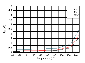
 Figure 6-42 Shutdown Current vs Temperature


