SLUSF98 November 2024 TPSM84338
PRODUCTION DATA
- 1
- 1 Features
- 2 Applications
- 3 Description
- 4 Pin Configuration and Functions
- 5 Specifications
-
6 Detailed Description
- 6.1 Overview
- 6.2 Functional Block Diagram
- 6.3
Feature Description
- 6.3.1 Fixed Frequency Peak Current Mode
- 6.3.2 Mode Selection
- 6.3.3 Voltage Reference
- 6.3.4 Output Voltage Setting
- 6.3.5 Switching Frequency Selection, Synchronization
- 6.3.6 Phase Shift
- 6.3.7 Enable and Adjusting Undervoltage Lockout
- 6.3.8 External Soft Start and Prebiased Soft Start
- 6.3.9 Power Good
- 6.3.10 Minimum On Time, Minimum Off Time, and Frequency Foldback
- 6.3.11 Frequency Spread Spectrum
- 6.3.12 Overvoltage Protection
- 6.3.13 Overcurrent and Undervoltage Protection
- 6.3.14 Thermal Shutdown
- 6.4 Device Functional Modes
-
7 Application and Implementation
- 7.1
Typical Application
- 7.1.1 Design Requirements
- 7.1.2
Detailed Design Procedure
- 7.1.2.1 Custom Design With WEBENCH® Tools
- 7.1.2.2 Output Voltage Resistors Selection
- 7.1.2.3 Choosing Switching Frequency
- 7.1.2.4 Soft-Start Capacitor Selection
- 7.1.2.5 Output Capacitor Selection
- 7.1.2.6 Input Capacitor Selection
- 7.1.2.7 Feedforward Capacitor CFF Selection
- 7.1.2.8 Maximum Ambient Temperature
- 7.1.3 Application Curves
- 7.2 Best Design Practices
- 7.3 Power Supply Recommendations
- 7.4 Layout
- 7.1
Typical Application
- 8 Device and Documentation Support
- 9 Revision History
- 10Mechanical, Packaging, and Orderable Information
Package Options
Mechanical Data (Package|Pins)
- RCJ|9
Thermal pad, mechanical data (Package|Pins)
Orderable Information
6.3.11 Frequency Spread Spectrum
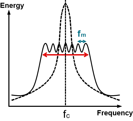
To reduce EMI, the TPSM84338 introduces frequency spread spectrum. The jittering span is typically Δfc = ±8% of the switching frequency with the modulation frequency of 10kHz. The purpose of spread spectrum is to eliminate peak emissions at specific frequencies by spreading emissions across a wider range of frequencies than a part with fixed frequency operation. Figure 6-7 shows the frequency spread spectrum modulation. Figure 6-8 shows the energy is spread out at the center frequency, fc.
 Figure 6-7 Frequency Spread Spectrum
Diagram
 Figure 6-8 Energy vs Frequency