SBOS971 December   2023 TRF1305B2

PRODUCTION DATA  

  1.   1
  2. Features
  3. Applications
  4. Description
  5. Device Comparison
  6. Pin Configuration and Functions
  7. Specifications
    1. 6.1 Absolute Maximum Ratings
    2. 6.2 ESD Ratings
    3. 6.3 Recommended Operating Conditions
    4. 6.4 Thermal Information
    5. 6.5 Electrical Characteristics - TRF1305B2
    6. 6.6 Typical Characteristics - TRF1305B2
  8. Detailed Description
    1. 7.1 Overview
    2. 7.2 Functional Block Diagram
    3. 7.3 Feature Description
      1. 7.3.1 Fully Differential Amplifier
      2. 7.3.2 Output Common-Mode Control
      3. 7.3.3 Internal Resistor Configuration
    4. 7.4 Device Functional Modes
      1. 7.4.1 MODE Pin
        1. 7.4.1.1 Input Common-Mode Extension
      2. 7.4.2 Power-Down Mode
  9. Application and Implementation
    1. 8.1 Application Information
      1. 8.1.1 Input and Output Interface Considerations
        1. 8.1.1.1 Single-Ended Input
        2. 8.1.1.2 Differential Input
        3. 8.1.1.3 DC Coupling Considerations
      2. 8.1.2 Gain Adjustment With External Resistors in a Differential Input Configuration
    2. 8.2 Typical Application
      1. 8.2.1 TRF1305x2 as ADC Driver in a Zero-IF Receiver
        1. 8.2.1.1 Design Requirements
        2. 8.2.1.2 Detailed Design Procedure
        3. 8.2.1.3 Application Curves
    3. 8.3 Power Supply Recommendations
      1. 8.3.1 Supply Voltages
      2. 8.3.2 Single-Supply Operation
      3. 8.3.3 Split-Supply Operation
      4. 8.3.4 Supply Decoupling
    4. 8.4 Layout
      1. 8.4.1 Layout Guidelines
        1. 8.4.1.1 Thermal Considerations
      2. 8.4.2 Layout Example
  10. Device and Documentation Support
    1. 9.1 Receiving Notification of Documentation Updates
    2. 9.2 Support Resources
    3. 9.3 Trademarks
    4. 9.4 Electrostatic Discharge Caution
    5. 9.5 Glossary
  11. 10Revision History
  12. 11Mechanical, Packaging, and Orderable Information

Package Options

Refer to the PDF data sheet for device specific package drawings

Mechanical Data (Package|Pins)
  • RYP|16
Thermal pad, mechanical data (Package|Pins)
Orderable Information

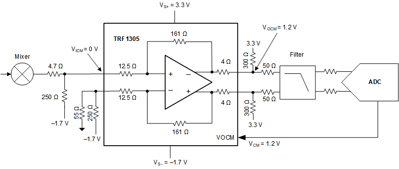
TRF1305x2 as ADC Driver in a Zero-IF Receiver

GUID-20221012-SS0I-T1WN-RRMD-ZS2CVJHSFVQQ-low.gif Figure 8-6 TRF1305x2 as ADC Driver in a Zero-IF Receiver

Consider a zero-IF (direct down conversion) application in which an IQ demodulator is interfaced to a pair of ADCs. The TRF1305x2 is used here as an interface amplifier between the demodulator and the ADCs. The dc common-mode of the demodulator output and ADC input are different. The TRF1305x2 dc couples the demodulator to ADC without degrading the signal integrity of the signal chain.