SBOS971 December   2023 TRF1305B2

PRODUCTION DATA  

  1.   1
  2. Features
  3. Applications
  4. Description
  5. Device Comparison
  6. Pin Configuration and Functions
  7. Specifications
    1. 6.1 Absolute Maximum Ratings
    2. 6.2 ESD Ratings
    3. 6.3 Recommended Operating Conditions
    4. 6.4 Thermal Information
    5. 6.5 Electrical Characteristics - TRF1305B2
    6. 6.6 Typical Characteristics - TRF1305B2
  8. Detailed Description
    1. 7.1 Overview
    2. 7.2 Functional Block Diagram
    3. 7.3 Feature Description
      1. 7.3.1 Fully Differential Amplifier
      2. 7.3.2 Output Common-Mode Control
      3. 7.3.3 Internal Resistor Configuration
    4. 7.4 Device Functional Modes
      1. 7.4.1 MODE Pin
        1. 7.4.1.1 Input Common-Mode Extension
      2. 7.4.2 Power-Down Mode
  9. Application and Implementation
    1. 8.1 Application Information
      1. 8.1.1 Input and Output Interface Considerations
        1. 8.1.1.1 Single-Ended Input
        2. 8.1.1.2 Differential Input
        3. 8.1.1.3 DC Coupling Considerations
      2. 8.1.2 Gain Adjustment With External Resistors in a Differential Input Configuration
    2. 8.2 Typical Application
      1. 8.2.1 TRF1305x2 as ADC Driver in a Zero-IF Receiver
        1. 8.2.1.1 Design Requirements
        2. 8.2.1.2 Detailed Design Procedure
        3. 8.2.1.3 Application Curves
    3. 8.3 Power Supply Recommendations
      1. 8.3.1 Supply Voltages
      2. 8.3.2 Single-Supply Operation
      3. 8.3.3 Split-Supply Operation
      4. 8.3.4 Supply Decoupling
    4. 8.4 Layout
      1. 8.4.1 Layout Guidelines
        1. 8.4.1.1 Thermal Considerations
      2. 8.4.2 Layout Example
  10. Device and Documentation Support
    1. 9.1 Receiving Notification of Documentation Updates
    2. 9.2 Support Resources
    3. 9.3 Trademarks
    4. 9.4 Electrostatic Discharge Caution
    5. 9.5 Glossary
  11. 10Revision History
  12. 11Mechanical, Packaging, and Orderable Information

Package Options

Refer to the PDF data sheet for device specific package drawings

Mechanical Data (Package|Pins)
  • RYP|16
Thermal pad, mechanical data (Package|Pins)
Orderable Information

Output Common-Mode Control

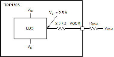
Figure 7-1 shows a functional diagram of the output common-mode control. Internally the VOCM pin sees an LDO output voltage that is equal to VS– + 2.5 V connected through a 2.5‑kΩ resistor.

Floating the VOCM pin is allowed. The output common-mode voltage at the output pins, OUTPx and OUTMx, defaults to the LDO output voltage of VS– + 2.5 V when VOCM pin is floated. Floating the VOCM pin results in a VOCM voltage equal to midsupply when VS = 5 V. If the VOCM pin is driven, then drive the pin from a low-impedance source. Limit the value of ROCM to less than 25 Ω for accurate reflection of the forced VOCM voltage at the device outputs.
GUID-20220924-SS0I-NV9B-KJBF-VZL50NK95Q0D-low.gif Figure 7-1 Output Common-Mode Control