SLLS822C July 2007 – December 2024 TRSF3221E
PRODUCTION DATA
- 1
- 1 Features
- 2 Applications
- 3 Description
- 4 Pin Configuration and Functions
-
5 Specifications
- 5.1 Absolute Maximum Ratings
- 5.2 ESD Ratings
- 5.3 ESD Ratings, IEC Specifications
- 5.4 Recommended Operating Conditions
- 5.5 Thermal Resistance Characteristics
- 5.6 Electrical Characteristics
- 5.7 Electrical Characteristics, Driver
- 5.8 Switching Characteristics, Driver
- 5.9 Electrical Characteristics, Receiver
- 5.10 Switching Characteristics, Receiver
- 5.11 Electrical Characteristics, Auto-Powerdown
- 5.12 Switching Characteristics, Auto-Powerdown
- 5.13 Typical Characteristics
- 6 Parameter Measurement Information
- 7 Detailed Description
- 8 Application and Implementation
- 9 Device and Documentation Support
- 10Revision History
- 11Mechanical, Packaging, and Orderable Information
Package Options
Mechanical Data (Package|Pins)
Thermal pad, mechanical data (Package|Pins)
- RGT|16
Orderable Information
4 Pin Configuration and Functions
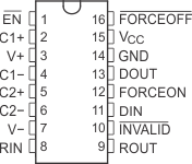
 DB or PW Package. 16 Pins (Top View)
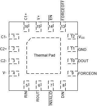
 RGT, VSON Package, 16 Pins (Top View)
Table 4-1 Pin Functions
| PIN | TYPE(1) | DESCRIPTION | ||
|---|---|---|---|---|
| NAME | DB or PW | RGT | ||
| EN | 1 | 14 | -- | Low input enables receiver ROUT output. High input sets ROUT to high impedance. |
| C1+ | 2 | 16 | - | Positive lead of C1 capacitor |
| V+ | 3 | 15 | O | Positive charge pump output for storage capacitor only |
| C1- | 4 | 1 | - | Negative lead of C1 capacitor |
| C2+ | 5 | 2 | - | Positive lead of C2 capacitor |
| C2- | 6 | 3 | - | Negative lead of C2 capacitor |
| V- | 7 | 4 | O | Negative charge pump output for storage capacitor only |
| RIN | 8 | 5 | I | RS232 line data input (from remote RS232 system) |
| ROUT | 9 | 6 | O | Logic data output (to UART) |
| INVALID | 10 | 7 | Invalid output pin. Output low when RIN input is unpowered. | |
| DIN | 11 | 8 | I | Logic data input (from UART) |
| FORCEON | 12 | 9 | Automatic power-down control input | |
| DOUT | 13 | 10 | O | RS232 line data output (to remote RS232 system) |
| GRD | 14 | 11 | - | Ground |
| VCC | 15 | 12 | - | Supply Voltage, Connect to external 3V to 5.5V power supply |
| FORCEOFF | 16 | 13 | Automatic power-down control input | |
| Thermal Pad | - | Yes | - | Exposed thermal pad. Can be connected to GND or left floating. |
(1) Signal Types: I = Input, O =
Output, I/O = Input or Output.
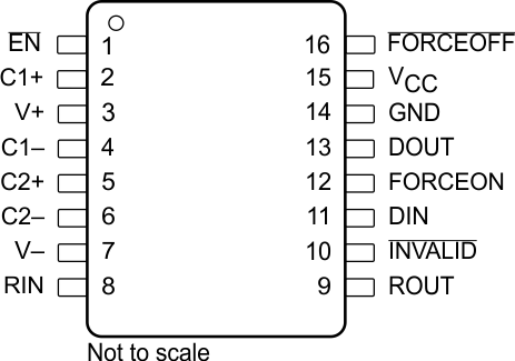
 Figure 4-1 DYY Package
16-Pin SOT-23-THN
(Top View)
Table 4-2 Pin Functions
| PIN | TYPE | DESCRIPTION | |
|---|---|---|---|
| NAME | NO. | ||
| EN | 1 | I | Low input enables receiver ROUT output. High input sets ROUT to high impedance. |
| C1+ | 2 | — | Positive terminals of the voltage-doubler charge pump capacitors |
| V+ | 3 | O | 5.5V supply generated by the charge pump |
| C1– | 4 | — | Negative terminals of the voltage-doubler charge pump capacitors |
| C2+ | 5 | Positive terminals of the voltage-doubler charge pump capacitors | |
| C2– | 6 | Negative terminals of the voltage-doubler charge pump capacitors | |
| V– | 7 | O | –5.5V supply generated by the charge pump |
| RIN | 8 | I | RS-232 receiver input |
| ROUT | 9 | O | Receiver output |
| INVALID | 10 | O | Invalid output pin. Output low when RIN input is unpowered. |
| DIN | 11 | I | Driver input |
| FORCEON | 12 | I | Automatic power-down control input |
| DOUT | 13 | O | RS-232 driver output |
| GND | 14 | — | Ground |
| VCC | 15 | — | 3V to 5.5V supply voltage |
| FORCEOFF | 16 | I | Automatic power-down control input |