SCDS337F December   2012  – June 2019 TS3USB3000

PRODUCTION DATA.  

  1. Features
  2. Applications
  3. Description
    1.     Device Images
      1.      Functional Block Diagram
  4. Revision History
  5. Pin Configuration and Functions
    1.     Pin Functions
  6. Specifications
    1. 6.1 Absolute Maximum Ratings
    2. 6.2 ESD Ratings
    3. 6.3 Recommended Operating Conditions
    4. 6.4 Thermal Information
    5. 6.5 Electrical Characteristics
    6. 6.6 Dynamic Characteristics
    7. 6.7 Timing Requirements
    8. 6.8 Typical Characteristics
  7. Parameter Measurement Information
  8. Detailed Description
    1. 8.1 Overview
    2. 8.2 Functional Block Diagram
    3. 8.3 Feature Description
      1. 8.3.1 Low Power Mode
      2. 8.3.2 Overvoltage Protection When 9-V Short to D+/– Pin
      3. 8.3.3 Pin Leakage
    4. 8.4 Device Functional Modes
      1. 8.4.1 High Impedance Mode
  9. Application and Implementation
    1. 9.1 Application Information
    2. 9.2 Typical Application
      1. 9.2.1 Design Requirements
      2. 9.2.2 Detailed Design Procedure
      3. 9.2.3 Application Curves
  10. 10Power Supply Recommendations
  11. 11Layout
    1. 11.1 Layout Guidelines
    2. 11.2 Layout Example
  12. 12Device and Documentation Support
    1. 12.1 Documentation Support
      1. 12.1.1 Related Documentation
    2. 12.2 Receiving Notification of Documentation Updates
    3. 12.3 Community Resources
    4. 12.4 Trademarks
    5. 12.5 Electrostatic Discharge Caution
    6. 12.6 Glossary
  13. 13Mechanical, Packaging, and Orderable Information
    1. 13.1 Package Option Addendum
      1. 13.1.1 Packaging Information

Package Options

Mechanical Data (Package|Pins)
Thermal pad, mechanical data (Package|Pins)
Orderable Information

Application Curves

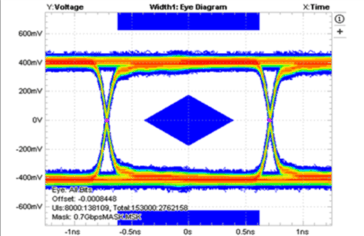
TS3USB3000 G001_a_cds337.gif
Figure 16. Eye Pattern: 0.7 Gbps With No Device
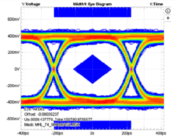
TS3USB3000 G002_a_cds337.gif
The TS3USB3000 contributes only 8.4 ps of peak-to-peak jitter for 0.7-Gbps data rate
Figure 18. Eye Pattern: 0.7 Gbps for MHL Switch
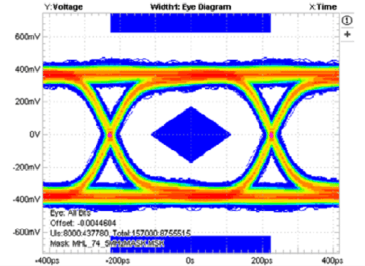
TS3USB3000 G003_a_cds337.gif
Figure 20. Eye Pattern: 2.2 Gbps With No Device
TS3USB3000 G004_a_cds337.gif
The TS3USB3000 contributes only 3.8 ps of peak-to-peak jitter for 2.2-Gbps data rate
Figure 22. Eye Pattern: 2.2 Gbps for MHL Switch
TS3USB3000 G005_a_cds337.gif
Figure 24. Eye Pattern: 3 Gbps With No Device
TS3USB3000 G006_a_cds337.gif
The TS3USB3000 contributes only 5.8 ps of peak-to-peak jitter for 3-Gbps data rate
Figure 26. Eye Pattern: 3 Gbps for MHL Switch
TS3USB3000 G007_a_cds337.gif
Figure 28. Eye Pattern: 4.5 Gbps With No Device
TS3USB3000 G008_a_cds337.gif
The TS3USB3000 contributes only 7.6 ps of peak-to-peak jitter for 4.5-Gbps data rate
Figure 30. Eye Pattern: 4.5 Gbps for MHL Switch
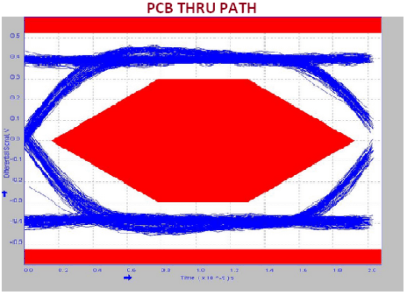
TS3USB3000 eye001_cds337.gif
Figure 32. 480-Mbps USB 2.0 Eye Pattern With No Device
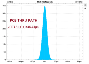
TS3USB3000 G001_b_cds337.gifFigure 17. Time Interval Error Histogram: 0.7 Gbps With No Device
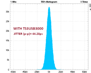
TS3USB3000 G002_b_cds337.gif
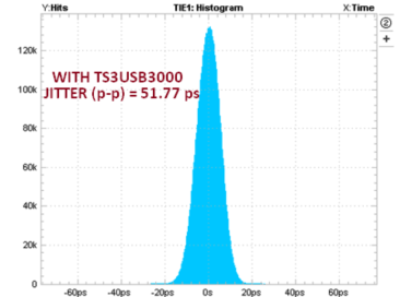
The TS3USB3000 contributes only 8.4 ps of peak-to-peak jitter for 0.7-Gbps data rate
Figure 19. Time Interval Error Histogram: 0.7 Gbps for MHL Switch
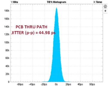
TS3USB3000 G003_b_cds337.gifFigure 21. Time Interval Error Histogram: 2.2 Gbps With No Device
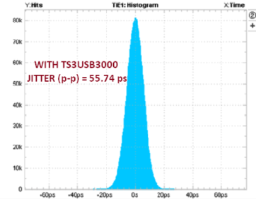
TS3USB3000 G004_b_cds337.gif
The TS3USB3000 contributes only 3.8 ps of peak-to-peak jitter for 2.2-Gbps data rate
Figure 23. Time Interval Error Histogram: 2.2 Gbps for MHL Switch
TS3USB3000 G005_b_cds337.gifFigure 25. Time Interval Error Histogram: 3 Gbps With No Device
TS3USB3000 G006_b_cds337.gif
The TS3USB3000 contributes only 5.8 ps of peak-to-peak jitter for 3-Gbps data rate
Figure 27. Time Interval Error Histogram: 3 Gbps for MHL Switch
TS3USB3000 G007_b_cds337.gif
Figure 29. Time Interval Error Histogram: 4.5 Gbps With No Device
TS3USB3000 G008_b_cds337.gif
The TS3USB3000 contributes only 7.6 ps of peak-to-peak jitter for 4.5-Gbps data rate
Figure 31. Time Interval Error Histogram: 4.5 Gbps for MHL Switch
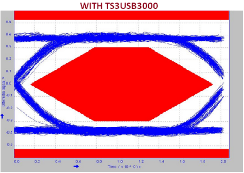
TS3USB3000 eye002_cds337.gif
Figure 33. 480-Mbps USB 2.0 Eye Pattern for USB Switch