SCDS361A October 2014 – July 2016 TS5A22364-Q1
PRODUCTION DATA.
- 1 Features
- 2 Applications
- 3 Description
- 4 Revision History
- 5 Pin Configuration and Functions
- 6 Specifications
- 7 Parameter Measurement Information
- 8 Detailed Description
- 9 Application and Implementation
- 10Power Supply Recommendations
- 11Layout
- 12Device and Documentation Support
- 13Mechanical, Packaging, and Orderable Information
Package Options
Mechanical Data (Package|Pins)
- DGS|10
Thermal pad, mechanical data (Package|Pins)
Orderable Information
9 Application and Implementation
NOTE
Information in the following applications sections is not part of the TI component specification, and TI does not warrant its accuracy or completeness. TI’s customers are responsible for determining suitability of components for their purposes. Customers should validate and test their design implementation to confirm system functionality.
9.1 Application Information
9.1.1 Negative Signal Swing Capability
The TS5A22364-Q1 dual SPDT switches feature negative signal capability that allows signals below ground to pass through without distortion. These analog switches operate from a single 2.3-V to 5.5-V supply. The input and output signal swing of the device is dependant on the supply voltage VCC: the device can pass signals as high as VCC and as low as VCC – 5.5 V, including signals below ground with minimal distortion. The Off state signal path (either NC or NO) during the operation of the TS5A22364-Q1 cannot handle negative DC voltage.
Table 2 shows the input-output signal swing the user can get with different supply voltages.
Table 2. Input-Output Signal Swing
| SUPPLY VOLTAGE, VCC | MINIMUM (VNC, VNO, VCOM) = VCC – 5.5 |
MAXIMUM (VNC, VNO, VCOM) = VCC |
MINIMUM (VNC, VNO, VCOM) = VCC – 5.5 |
MAXIMUM (VNC, VNO, VCOM) = VCC |
|---|---|---|---|---|
| ON State signal path | OFF state signal path | |||
| 5.5 V | 0 V | 5.5 V | 0 V | 5.5 V |
| 4.2 V | –1.3 V | 4.2 V | 0 V | 4.2 V |
| 3.3 V | –2.2 V | 3.3 V | 0 V | 3.3 V |
| 3 V | –2.5 V | 3 V | 0 V | 3 V |
| 2.5 V | –3 V | 2.5 V | 0 V | 2.5 V |
9.2 Typical Application
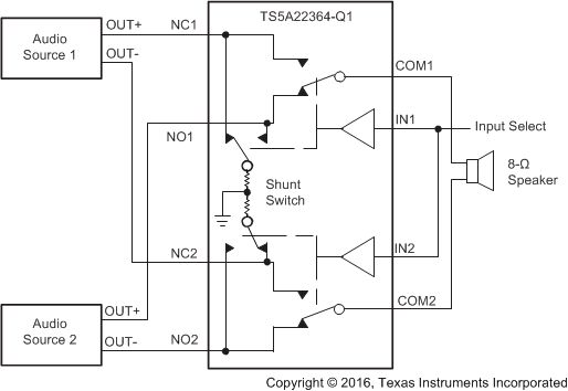
The 50-Ω shunt switches on the TS5A22364-Q1 automatically discharge any capacitance at the NC or NO terminals when they are unconnected to COM. This reduces audible click-and-pop sounds that occur when switching between audio sources. Audible clicks and pops are caused when a step DC voltage is switched into the speaker. By automatically discharging the side that is not connected, any residual DC voltage is removed, thereby reducing the clicks and pops. See Figure 25.
 Figure 25. Shunt Switch Block Diagram
9.2.1 Design Requirements
Tie the digitally controlled input select pins IN1 and IN2 to VCC or GND to avoid unwanted switch states that could result if the logic control pins are left floating.
9.2.2 Detailed Design Procedure
Select the appropriate supply voltage to cover the entire voltage swing of the signal passing through the switch because the TS5A22364-Q1 operates from a single 2.3-V to 5.5-V supply and the input-output signal swing of the device is dependant of the supply voltage VCC. The device passes signals as high as VCC and as low as VCC – 5.5 V. Use Table 2 as a guide for selecting supply voltage based on the signal passing through the switch.
Limit the current through the shunt resistor so as not to exceed the ±20 mA.
Ensure that the device is powered up with a supply voltage on VCC before a voltage can be applied to the signal paths NC and NO.
9.2.3 Application Curve
 Figure 26. On-Resistance vs Voltage VCOM