SCDS377B March 2018 – June 2018 TS5USBC41
PRODUCTION DATA.
- 1 Features
- 2 Applications
- 3 Description
- 4 Revision History
- 5 Pin Configuration and Functions
- 6 Specifications
- 7 Parameter Measurement Information
- 8 Detailed Description
- 9 Application and Implementation
- 10Power Supply Recommendations
- 11Layout
- 12Device and Documentation Support
- 13Mechanical, Packaging, and Orderable Information
Package Options
Refer to the PDF data sheet for device specific package drawings
Mechanical Data (Package|Pins)
- YFF|12
Thermal pad, mechanical data (Package|Pins)
Orderable Information
7 Parameter Measurement Information

Channel ON, RON = V/ISINK
Figure 5. ON-State Resistance (RON)
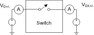 Figure 6. Off Leakage
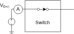 Figure 7. On Leakage
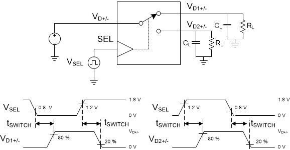
1. All input pulses are supplied by generators having the following characteristics: PRR ≤ 10 MHz, ZO = 50 Ω, tr< 500 ps, tf< 500 ps.
2. CL includes probe and jig capacitance.
Figure 8. tSWITCH Timing

1. All input pulses are supplied by generators having the following characteristics: PRR = 10 MHz, ZO = 50 Ω, tr< 500 ps, tf< 500 ps.
2. CL includes probe and jig capacitance.
Figure 9. tON, tOFF for OE
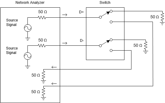 Figure 10. Off Isolation
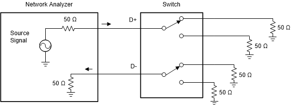 Figure 11. Cross Talk
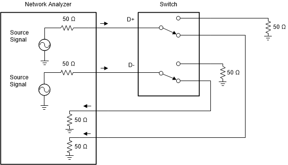 Figure 12. BW and Insertion Loss

1. All input pulses are supplied by generators having the following characteristics: PRR = 240 MHz, ZO = 50 Ω, tr< 500 ps, tf< 500 ps.
2. CL includes probe and jig capacitance.
Figure 14. tPD

1. All input pulses are supplied by generators having the following characteristics: PRR ≤ 10 MHz, ZO = 50 Ω, tr< 500 ps, tf< 500 ps.
2. CL includes probe and jig capacitance.
Figure 15. tSK
