SCDS377B March   2018  – June 2018 TS5USBC41

PRODUCTION DATA.  

  1. Features
  2. Applications
  3. Description
    1.     Device Images
      1.      Simplified Schematic
  4. Revision History
  5. Pin Configuration and Functions
    1.     Pin Functions
  6. Specifications
    1. 6.1 Absolute Maximum Ratings
    2. 6.2 ESD Ratings
    3. 6.3 Recommended Operating Conditions
    4. 6.4 Thermal Information
    5. 6.5 Electrical Characteristics
    6. 6.6 Dynamic Characteristics
    7. 6.7 Timing Requirements
    8. 6.8 Typical Characteristics
  7. Parameter Measurement Information
  8. Detailed Description
    1. 8.1 Overview
    2. 8.2 Functional Block Diagram
    3. 8.3 Feature Description
      1. 8.3.1 Powered-off Protection
      2. 8.3.2 Overvoltage Protection
    4. 8.4 Device Functional Modes
      1. 8.4.1 Pin Functions
  9. Application and Implementation
    1. 9.1 Application Information
    2. 9.2 Typical Application
      1. 9.2.1 Design Requirements
      2. 9.2.2 Detailed Design Procedure
      3. 9.2.3 Application Curves
  10. 10Power Supply Recommendations
  11. 11Layout
    1. 11.1 Layout Guidelines
    2. 11.2 Layout Example
  12. 12Device and Documentation Support
    1. 12.1 Documentation Support
      1. 12.1.1 Related Documentation
    2. 12.2 Receiving Notification of Documentation Updates
    3. 12.3 Community Resources
    4. 12.4 Trademarks
    5. 12.5 Electrostatic Discharge Caution
    6. 12.6 Glossary
  13. 13Mechanical, Packaging, and Orderable Information

Package Options

Refer to the PDF data sheet for device specific package drawings

Mechanical Data (Package|Pins)
  • YFF|12
Thermal pad, mechanical data (Package|Pins)
Orderable Information

Typical Characteristics

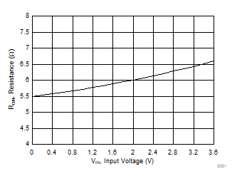
TS5USBC41 D001_SCDS369.gif
VCC = 3.3 V TA = 25°C
Figure 1. ON-Resistance vs Input Voltage
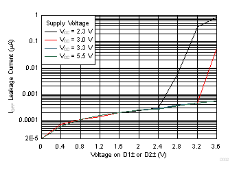
TS5USBC41 D002_SCDS372.gif
Figure 3. IOFF Leakage Current vs Voltage on D1± or D2±
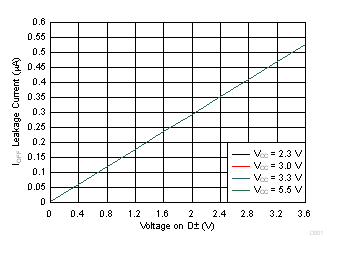
TS5USBC41 D001_SCDS372.gif
Figure 2. IOFF Leakage Current vs Voltage on D±
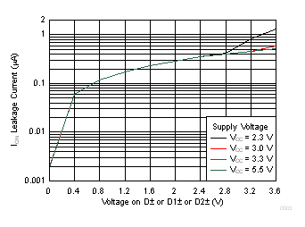
TS5USBC41 D003_SCDS372.gif
Figure 4. ION Leakage Current vs Voltage on D± or D1± or D2±