SBAS545A September 2011 – December 2016 TSC2007-Q1
PRODUCTION DATA.
- 1 Features
- 2 Applications
- 3 Description
- 4 Revision History
- 5 Pin Configuration and Functions
-
6 Specifications
- 6.1 Absolute Maximum Ratings
- 6.2 ESD Ratings
- 6.3 Recommended Operating Conditions
- 6.4 Thermal Information
- 6.5 Electrical Characteristics
- 6.6 Timing Requirements: Standard Mode (SCL = 100 kHz)
- 6.7 Timing Requirements: Fast Mode (SCL = 400 kHz)
- 6.8 Timing Requirements: High-Speed Mode (SCL = 1.7 MHz)
- 6.9 Timing Requirements: High-Speed Mode (SCL = 3.4 MHz)
- 6.10 Typical Characteristics
- 7 Detailed Description
- 8 Application and Implementation
- 9 Power Supply Recommendations
- 10Layout
- 11Device and Documentation Support
- 12Mechanical, Packaging, and Orderable Information
Package Options
Mechanical Data (Package|Pins)
- PW|16
Thermal pad, mechanical data (Package|Pins)
Orderable Information
6 Specifications
6.1 Absolute Maximum Ratings
Over operating free-air temperature range (unless otherwise noted).(1)| MIN | MAX | UNIT | ||
|---|---|---|---|---|
| Analog input voltage | X+, Y+, AUX to GND | –0.4 | VDD + 0.1 | V |
| X–, Y– to GND | –0.4 | VDD + 0.1 | ||
| Voltage | VDD/REF pin to GND | –0.3 | 5 | V |
| Digital input voltage to GND | –0.3 | VDD + 0.3 | V | |
| Digital output voltage to GND | –0.3 | VDD + 0.3 | V | |
| Power dissipation | (TJ(MAX) – TA) / RθJA | |||
| Operating free-air temperature, TA | –40 | 85 | °C | |
| Junction temperature, TJ | 150 | °C | ||
| Storage temperature, Tstg | –65 | 150 | °C | |
(1) Stresses beyond those listed under Absolute Maximum Ratings may cause permanent damage to the device. These are stress ratings only, which do not imply functional operation of the device at these or any other conditions beyond those indicated under Recommended Operating Conditions. Exposure to absolute-maximum-rated conditions for extended periods may affect device reliability.
6.2 ESD Ratings
| VALUE | UNIT | ||||
|---|---|---|---|---|---|
| V(ESD) | Electrostatic discharge | Human-body model (HBM), per AEC Q100-002(1) | ±8000 | V | |
| Charged-device model (CDM), per AEC Q100-011 | ±1000 | ||||
| IEC 61000-4-2 contact discharge(2) | Pins 2, 3, 4, and 5 | ±15000 | |||
| IEC 61000-4-2 air-gap discharge(2) | Pins 2, 3, 4, and 5 | ±25000 | |||
(1) AEC Q100-002 indicates that HBM stressing shall be in accordance with the ANSI/ESDA/JEDEC JS-001 specification.
(2) Test method based on IEC standard 61000-4-2. Contact Texas Instruments for test details.
6.3 Recommended Operating Conditions
over operating free-air temperature range (unless otherwise noted)| MIN | MAX | UNIT | |||
|---|---|---|---|---|---|
| VDD | Power-supply voltage | VDD | 1.2 | 3.6 | V |
6.4 Thermal Information
| THERMAL METRIC(1) | TSC2007-Q1 | UNIT | |
|---|---|---|---|
| PW (TSSOP) | |||
| 16 PINS | |||
| RθJA | Junction-to-ambient thermal resistance | 101.7 | °C/W |
| RθJC(top) | Junction-to-case (top) thermal resistance | 35.2 | °C/W |
| RθJB | Junction-to-board thermal resistance | 47.7 | °C/W |
| ψJT | Junction-to-top characterization parameter | 2.4 | °C/W |
| ψJB | Junction-to-board characterization parameter | 47 | °C/W |
(1) For more information about traditional and new thermal metrics, see the Semiconductor and IC Package Thermal Metrics application report.
6.5 Electrical Characteristics
TA = –40°C to 85°C, VDD = 1.2 V to 3.6 V (unless otherwise noted).| PARAMETER | TEST CONDITIONS | MIN | TYP | MAX | UNIT | ||
|---|---|---|---|---|---|---|---|
| AUXILIARY ANALOG INPUT | |||||||
| Input voltage range | 0 | VDD | V | ||||
| Input capacitance | 12 | pF | |||||
| Input leakage current | –1 | 1 | µA | ||||
| A-D CONVERTER | |||||||
| Resolution | Programmable: 8 bits or 12 bits | 12 | Bits | ||||
| No missing codes | 12-bit resolution | 11 | Bits | ||||
| Integral linearity | ±1.5 | LSB(1) | |||||
| Offset error | VDD = 1.8 V | –1.2 | LSB | ||||
| VDD = 3 V | –3.1 | LSB | |||||
| Gain error | VDD = 1.8 V | 0.7 | LSB | ||||
| VDD = 3 V | 0.1 | LSB | |||||
| TOUCH SENSORS | |||||||
| PENIRQ pullup resistor, RIRQ | TA = 25°C, VDD = 1.8 V, command 1011 set 0000 | 51 | kΩ | ||||
| TA = 25°C, VDD = 1.8 V, command 1011 set 0001 | 90 | kΩ | |||||
| Switch ON‑resistance | Y+, X+ | 6 | Ω | ||||
| Y–, X– | 5 | Ω | |||||
| Switch drivers drive current(5)(2) | 100-ms duration | 50 | mA | ||||
| INTERNAL TEMPERATURE SENSOR | |||||||
| Temperature range | –40 | 85 | °C | ||||
| Resolution | Differential method(3) | VDD = 3 V | 1.94 | °C/LSB | |||
| VDD = 1.6 V | 1.04 | °C/LSB | |||||
| TEMP1(4) | VDD = 3 V | 0.35 | °C/LSB | ||||
| VDD = 1.6 V | 0.19 | °C/LSB | |||||
| Accuracy | Differential method(3) | VDD = 3 V | ±2 | °C/LSB | |||
| VDD = 1.6 V | ±2 | °C/LSB | |||||
| TEMP1(4) | VDD = 3 V | ±3 | °C/LSB | ||||
| VDD = 1.6 V | ±3 | °C/LSB | |||||
| INTERNAL OSCILLATOR | |||||||
| Internal clock frequency, fCCLK | 8-Bit | VDD = 1.2 V | 3.19 | MHz | |||
| VDD = 1.8 V | 3.66 | MHz | |||||
| VDD = 2.7 V | 3.78 | MHz | |||||
| VDD = 3.6 V | 3.82 | MHz | |||||
| 12-Bit | VDD = 1.2 V | 1.6 | MHz | ||||
| VDD = 1.8 V | 1.83 | MHz | |||||
| VDD = 2.7 V | 1.88 | MHz | |||||
| VDD = 3.6 V | 1.91 | MHz | |||||
| Frequency drift | VDD = 1.6 V | 0.0056 | %/°C | ||||
| VDD = 3 V | 0.012 | %/°C | |||||
| DIGITAL INPUT AND OUTPUT | |||||||
| Logic family | CMOS | ||||||
| Logic level | VIH | 1.2 V ≤ VDD < 1.6 V | 0.7 × VDD | VDD + 0.3 | V | ||
| 1.6 V ≤ VDD ≤ 3.6 V | 0.7 × VDD | VDD + 0.3 | V | ||||
| VIL | 1.2 V ≤ VDD < 1.6 V | –0.3 | 0.2 × VDD | V | |||
| 1.6 V ≤ VDD ≤ 3.6 V | –0.3 | 0.3 × VDD | V | ||||
| IIL | SCL and SDA pins | –1 | 1 | µA | |||
| CIN(5) | SCL and SDA pins | 10 | pF | ||||
| VOH | IOH = 2 TTL loads | VDD – 0.2 | VDD | V | |||
| VOL | IOL = 2 TTL loads | 0 | 0.2 | V | |||
| ILEAK | Floating output | –1 | 1 | µA | |||
| COUT(5) | Floating output | 10 | pF | ||||
| Data format | Straight binary | ||||||
| POWER-SUPPLY REQUIREMENTS | |||||||
| Quiescent supply current (VDD with sensor off) |
12-bit Fast mode (clock = 400 kHz) PD[1:0] = 0,0 |
VDD = 1.2 V, 32.56k eq rate | 128 | 190 | µA | ||
| VDD = 1.2 V, 8.2k eq rate | 32.24 | µA | |||||
| VDD = 1.8 V, 34.42k eq rate | 165 | 240 | µA | ||||
| VDD = 1.8 V, 8.2k eq rate | 39.31 | µA | |||||
| VDD = 2.7 V, 34.79k eq rate | 226.2 | 335 | µA | ||||
| VDD = 2.7 V, 8.2k eq rate | 53.32 | µA | |||||
| Power down supply current | Not addressed, SCL = SDA = 1 | 0 | 0.8 | µA | |||
| POWER-ON AND OFF SLOPE REQUIREMENTS(5) | |||||||
| VDD off ramp | TA = –40°C to 85°C | 2 | kV/s | ||||
| VDD off time | TA = –40°C to 85°C, VDD = 0 V | 1.2 | s | ||||
| TA = –20°C to 85°C, VDD = 0 V | 0.3 | s | |||||
| VDD on ramp | TA = –40°C to 85°C | 12 | kV/s | ||||
(1) LSB means Least Significant Bit. With VDD/REF pin = 1.6 V, one LSB is 391 µV.
(2) Exceeding 50-mA source current may result in device degradation.
(3) Difference between TEMP1 and TEMP2 measurement; no calibration necessary.
(4) Temperature drift is –2.1 mV/°C.
(5) Not production tested. Specified by design.
6.6 Timing Requirements: Standard Mode (SCL = 100 kHz)
TA = –40°C to 85°C, VDD = 1.6 V (unless otherwise noted).| MIN | NOM | MAX | UNIT | ||||
|---|---|---|---|---|---|---|---|
| fSCL | SCL clock frequency | 0 | 100 | kHz | |||
| tBUF | Bus free time between a STOP and START condition | 4.7 | µs | ||||
| tHD, STA | Hold time (repeated) START condition | 4 | µs | ||||
| tLOW | Low period of SCL clock | 4.7 | µs | ||||
| tHIGH | High period of the SCL clock | 4 | µs | ||||
| tSU, STA | Setup time for a repeated START condition | 4.7 | µs | ||||
| tHD, DAT | Data hold time | 0 | 3.45 | µs | |||
| tSU, DAT | Data setup time | 250 | ns | ||||
| tR | Rise time for both SDA and SCL signals (receiving) | Cb = total bus capacitance | 1000 | ns | |||
| tF | Fall time for both SDA and SCL signals | Receiving | Cb = total bus capacitance | 300 | ns | ||
| Transmitting | Cb = total bus capacitance | 250 | ns | ||||
| tSU, STO | Setup time for STOP condition | 4 | µs | ||||
| Cb | Capacitive load for each bus line | Cb = total capacitance of one bus line in pF | 400 | pF | |||
| Cycle time | 8 bits | 40 SCL + 127 CCLK, VDD = 1.8 V | 434.7 | µs | |||
| 12 bits | 49 SCL + 148 CCLK, VDD = 1.8 V | 570.9 | µs | ||||
| Effective throughput | 8 bits | VDD = 1.8 V | 2.3 | kSPS | |||
| 12 bits | VDD = 1.8 V | 1.75 | kSPS | ||||
| Equivalent rate = effective throughput × 7 | 8 bits | VDD = 1.8 V | 16.1 | kHz | |||
| 12 bits | VDD = 1.8 V | 12.26 | kHz | ||||
6.7 Timing Requirements: Fast Mode (SCL = 400 kHz)
All specifications typical at –40°C to 85°C, VDD = 1.6 V (unless otherwise noted).| MIN | NOM | MAX | UNIT | ||||
|---|---|---|---|---|---|---|---|
| fSCL | SCL clock frequency | 0 | 400 | kHz | |||
| tBUF | Bus free time between a STOP and START condition | 1.3 | µs | ||||
| tHD, STA | Hold time (repeated) START condition | 0.6 | µs | ||||
| tLOW | Low period of SCL clock | 1.3 | µs | ||||
| tHIGH | High period of the SCL clock | 0.6 | µs | ||||
| tSU, STA | Setup time for a repeated START condition | 0.6 | µs | ||||
| tHD, DAT | Data hold time | 0 | 0.9 | µs | |||
| tSU, DAT | Data setup time | 100 | ns | ||||
| tR | Rise time for both SDA and SCL signals (receiving) | Cb = total bus capacitance | 20 + 0.1 × Cb | 300 | ns | ||
| tF | Fall time for both SDA and SCL signals | Receiving | Cb = total bus capacitance | 20 + 0.1 × Cb | 300 | ns | |
| Transmitting | Cb = total bus capacitance | 20 + 0.1 × Cb | 250 | ns | |||
| tSU, STO | Setup time for STOP condition | 0.6 | µs | ||||
| Cb | Capacitive load for each bus line | Cb = total capacitance of one bus line in pF | 400 | pF | |||
| Cycle time | 8 bits | 40 SCL + 127 CCLK, VDD = 1.8 V | 134.7 | µs | |||
| 12 bits | 49 SCL + 148 CCLK, VDD = 1.8 V | 203.4 | µs | ||||
| Effective throughput | 8 bits | VDD = 1.8 V | 7.42 | kSPS | |||
| 12 bits | VDD = 1.8 V | 4.92 | kSPS | ||||
| Equivalent rate = effective throughput × 7 | 8 bits | VDD = 1.8 V | 51.97 | kHz | |||
| 12 bits | VDD = 1.8 V | 34.42 | kHz | ||||
6.8 Timing Requirements: High-Speed Mode (SCL = 1.7 MHz)
All specifications typical at –40°C to 85°C, VDD = 1.6 V (unless otherwise noted).| MIN | NOM | MAX | UNIT | ||||
|---|---|---|---|---|---|---|---|
| fSCL | SCL clock frequency | 0 | 1.7 | MHz | |||
| tHD, STA | Hold time (repeated) START condition | 160 | ns | ||||
| tLOW | Low period of SCL clock | 320 | ns | ||||
| tHIGH | High period of the SCL clock | 120 | ns | ||||
| tSU, STA | Setup time for a repeated START condition | 160 | ns | ||||
| tHD, DAT | Data hold time | 0 | 150 | ns | |||
| tSU, DAT | Data setup time | 10 | ns | ||||
| tR | Rise time for a signal (receiving) | SCL | Cb = total bus capacitance | 20 | 80 | ns | |
| SDA | Cb = total bus capacitance | 20 | 160 | ns | |||
| tF | Fall time for a signal (receiving) | SCL | Cb = total bus capacitance | 20 | 80 | ns | |
| SDA | Cb = total bus capacitance | 20 | 160 | ns | |||
| tF | Fall time for both SDA and SCL signals (transmitting) | Cb = total bus capacitance | 20 | 160 | ns | ||
| tSU, STO | Setup time for STOP condition | 160 | ns | ||||
| Cb | Capacitive load for each bus line | Cb = total capacitance of one bus line in pF | 400 | pF | |||
| Cycle time | 8 bits | 40 SCL + 127 CCLK, VDD = 1.8 V | 58.2 | µs | |||
| 12 bits | 49 SCL + 148 CCLK, VDD = 1.8 V | 109.7 | µs | ||||
| Effective throughput | 8 bits | VDD = 1.8 V | 17.17 | kSPS | |||
| 12 bits | VDD = 1.8 V | 9.12 | kSPS | ||||
| Equivalent rate = effective throughput × 7 | 8 bits | VDD = 1.8 V | 120.22 | kHz | |||
| 12 bits | VDD = 1.8 V | 63.81 | kHz | ||||
6.9 Timing Requirements: High-Speed Mode (SCL = 3.4 MHz)
All specifications typical at –40°C to 85°C, VDD = 1.6 V (unless otherwise noted).| MIN | NOM | MAX | UNIT | ||||
|---|---|---|---|---|---|---|---|
| fSCL | SCL clock frequency | 0 | 3.4 | MHz | |||
| tHD, STA | Hold time (repeated) START condition | 160 | ns | ||||
| tLOW | Low period of SCL clock | 160 | ns | ||||
| tHIGH | High period of the SCL clock | 60 | ns | ||||
| tSU, STA | Setup time for a repeated START condition | 160 | ns | ||||
| tHD, DAT | Data hold time | 0 | 70 | ns | |||
| tSU, DAT | Data setup time | 10 | ns | ||||
| tR | Rise time for a signal (receiving) | SCL | Cb = total bus capacitance | 10 | 40 | ns | |
| SDA | Cb = total bus capacitance | 10 | 80 | ns | |||
| tF | Fall time for a signal (receiving) | SCL | Cb = total bus capacitance | 10 | 40 | ns | |
| SDA | Cb = total bus capacitance | 10 | 80 | ns | |||
| tF | Fall time for both SDA and SCL signals (transmitting) | Cb = total bus capacitance | 10 | 80 | ns | ||
| tSU, STO | Setup time for STOP condition | 160 | ns | ||||
| Cb | Capacitive load for each bus line | Cb = total capacitance of one bus line in pF | 100 | pF | |||
| Cycle time | 8 bits | 40 SCL + 127 CCLK, VDD = 1.8 V | 46.5 | µs | |||
| 12 bits | 49 SCL + 148 CCLK, VDD = 1.8 V | 95.3 | µs | ||||
| Effective throughput | 8 bits | VDD = 1.8 V | 21.52 | kSPS | |||
| 12 bits | VDD = 1.8 V | 10.49 | kSPS | ||||
| Equivalent rate = effective throughput × 7 | 8 bits | VDD = 1.8 V | 150.65 | kHz | |||
| 12 bits | VDD = 1.8 V | 73.46 | kHz | ||||
 Figure 1. Detailed I/O Timing
6.10 Typical Characteristics
At TA = –40°C to 85°C, VDD = 1.2 V to 3.6 V, PD1 = PD0 = 0, Fast mode, 12-bit mode, non-continuous AUX measurement, and MAV filter enabled (see MAV Filter section), unless otherwise noted.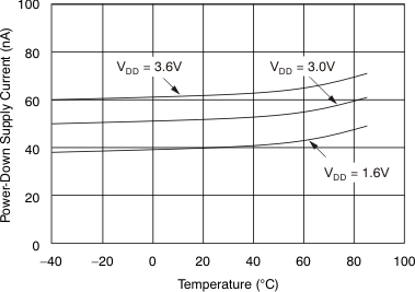 Figure 2. Power-Down Supply Current vs Temperature
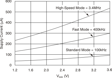 Figure 4. Supply Current vs
Supply Voltage (AUX Conversion)
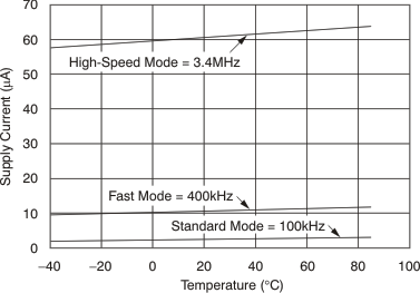 Figure 6. Supply Current (Part Not Addressed) vs Temperature
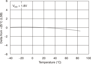 Figure 8. Change in Gain vs Temperature
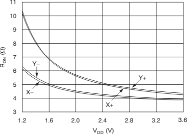 Figure 10. Switch ON-Resistance vs Supply Voltage
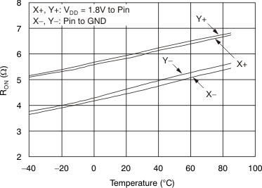 Figure 12. Switch ON-Resistance vs Temperature
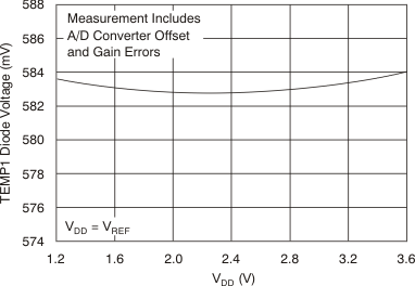 Figure 14. TEMP1 Diode Voltage vs Supply Voltage
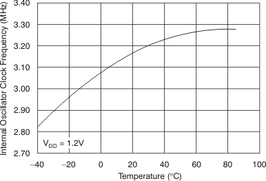 Figure 16. Internal Oscillator Clock Frequency vs Temperature
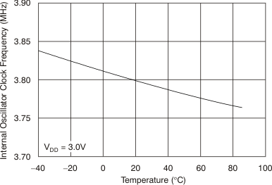 Figure 18. Internal Oscillator Clock Frequency vs Temperature
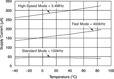 Figure 3. Supply Current vs Temperature
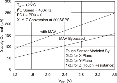 Figure 5. Supply Current vs Supply Voltage
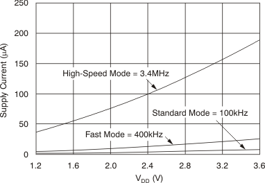 Figure 7. Supply Current (Part Not Addressed) vs
Supply Voltage
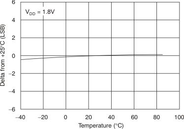 Figure 9. Change in Gain vs Temperature
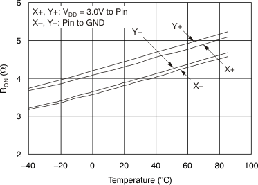 Figure 11. Switch ON-Resistance vs Temperature
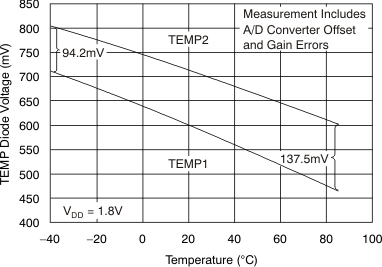 Figure 13. TEMP Diode Voltage vs Temperature
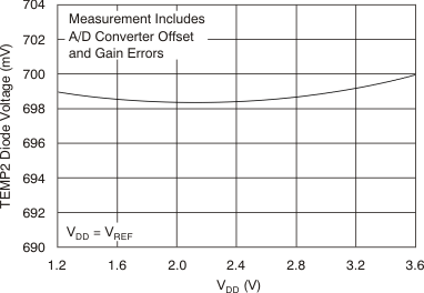 Figure 15. TEMP2 Diode Voltage vs Supply Voltage
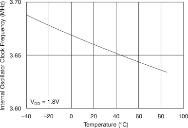 Figure 17. Internal Oscillator Clock Frequency vs Temperature