SLVSC89A June   2014  – July 2014 TSC2013-Q1

PRODUCTION DATA.  

  1. Features
  2. Applications
  3. Description
  4. Revision History
  5. Pin Configurations and Functions
  6. Specifications
    1. 6.1  Absolute Maximum Ratings
    2. 6.2  Handling Ratings
    3. 6.3  Recommended Operating Conditions
    4. 6.4  Thermal Information
    5. 6.5  Electrical Characteristics
    6. 6.6  Timing Requirements — I2C Standard Mode (ƒ(SCL) = 100 kHz)
    7. 6.7  Timing Requirements — I2C Fast Mode (ƒ(SCL) = 400 kHz)
    8. 6.8  Timing Requirements — I2C High-Speed Mode (ƒ(SCL) = 1.7 MHz)
    9. 6.9  Timing Requirements — I2C High-Speed Mode (ƒ(SCL) = 3.4 MHz)
    10. 6.10 Typical Characteristics
  7. Detailed Description
    1. 7.1 Overview
    2. 7.2 Functional Block Diagram
    3. 7.3 Feature Description
      1. 7.3.1 Touch-Screen Operation
      2. 7.3.2 4-Wire Touch Screen Measurements
      3. 7.3.3 Analog-to-Digital Converter
        1. 7.3.3.1 Data Format
        2. 7.3.3.2 Reference
        3. 7.3.3.3 Variable Resolution
        4. 7.3.3.4 Conversion Clock and Conversion Time
        5. 7.3.3.5 Touch Detect
        6. 7.3.3.6 Preprocessing
          1. 7.3.3.6.1 Preprocessing—Median Value Filter and Averaging Value Filter
    4. 7.4 Device Functional Modes
      1. 7.4.1 Conversion Controlled by TSC2013-Q1 and Initiated by TSC2013-Q1 (TSMode 1)
        1. 7.4.1.1 IX-IY Scan
        2. 7.4.1.2 X-Triplet, Y-Triplet, Z-Scan
      2. 7.4.2 Conversion Controlled by TSC2013-Q1 and Initiated by Host (TSMode 2)
      3. 7.4.3 Conversion Controlled by Host (TSMode 3)
    5. 7.5 Programming
      1. 7.5.1 I2C Interface
        1. 7.5.1.1 I2C Fast or Standard Mode (F-S Mode)
        2. 7.5.1.2 I2C High-Speed Mode (Hs Mode)
      2. 7.5.2 Digital Interface
        1. 7.5.2.1 Address Byte
      3. 7.5.3 Control Byte
        1. 7.5.3.1 Touch-Screen Scan Function for XYZ or XY
      4. 7.5.4 Start a Write Cycle
      5. 7.5.5 Register Access
      6. 7.5.6 Communication Protocol
      7. 7.5.7 Register Reset
    6. 7.6 Register Maps
      1. 7.6.1 Register Content and Reset Values
      2. 7.6.2 Configuration and Status Registers
        1. 7.6.2.1 Configuration Register 0
          1. 7.6.2.1.1 Configuration Register 0 (address = 0) [reset = 4000h for read; 0000h for write]
        2. 7.6.2.2 Configuration Register 1 (address = Dh) [reset = 0000h]
        3. 7.6.2.3 Configuration Register 2 (address = Eh) [reset = 0000h]
        4. 7.6.2.4 Converter-Function Select Register (address = Fh) [reset = 0000h]
        5. 7.6.2.5 Status Register (address = 8h) [reset = 0004h]
      3. 7.6.3 Data Registers
        1. 7.6.3.1 X1, X2, IX, Y1, Y2, IY, Z1, Z2, and AUX registers (offset = see ) [reset = see ]
  8. Application and Implementation
    1. 8.1 Application Information
      1. 8.1.1 Auxiliary Measurement
      2. 8.1.2 Single IX or Single IY Measurement
    2. 8.2 Typical Application
      1. 8.2.1 Design Requirements
      2. 8.2.2 Detailed Design Procedure
        1. 8.2.2.1 Power-On-Reset and Reset Consideration
          1. 8.2.2.1.1 Power-On Reset
          2. 8.2.2.1.2 Requesting a Minimal t(SNSVDD_OFF) Time
          3. 8.2.2.1.3 Requesting a Minimal t(SNSVDD_OFF_ramp) and t(SNSVDD_ON_ramp) Ramp
          4. 8.2.2.1.4 Hardware Reset
          5. 8.2.2.1.5 Software Reset
        2. 8.2.2.2 Power Up Considerations
          1. 8.2.2.2.1 Power-Off Cycles During Normal Operation
          2. 8.2.2.2.2 Supply Glitches During Normal Operation
          3. 8.2.2.2.3 TSC2013-Q1 Digital Pins
          4. 8.2.2.2.4 Suggested Hardware Reset During Power-On
        3. 8.2.2.3 Device Timing Setup and Use
          1. 8.2.2.3.1 Touch-Panel Driving Power
          2. 8.2.2.3.2 ADC Clock Effects
        4. 8.2.2.4 Panel Voltage Stabilization Time
        5. 8.2.2.5 Precharge and Sense Time
        6. 8.2.2.6 Single-Touch Operation
      3. 8.2.3 Application Curves
  9. Power Supply Recommendations
  10. 10Layout
    1. 10.1 Layout Guidelines
    2. 10.2 Layout Example
  11. 11Device and Documentation Support
    1. 11.1 Trademarks
    2. 11.2 Electrostatic Discharge Caution
    3. 11.3 Glossary
  12. 12Mechanical, Packaging, and Orderable Information

Package Options

Mechanical Data (Package|Pins)
Thermal pad, mechanical data (Package|Pins)
Orderable Information

5 Pin Configurations and Functions

16-Pin VQFN With Thermal Pad
RSA Package
Top View
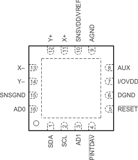
po_rsa_slvsc89.gif
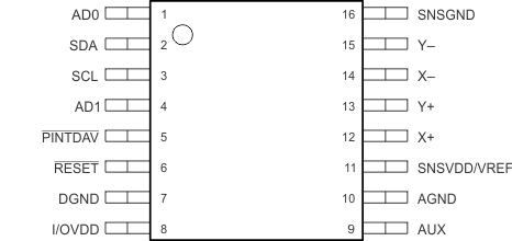
16-Pin TSSOP
PW Package
Top View
po_pw_slvsc89.gif

Pin Functions

PIN I/O ADC DESCRIPTION
NAME RSA PW
AD0 16 1 I D I2C bus TSC address input bit 0
AD1 3 4 I D I2C bus TSC address input bit 1
AGND 9 10 Analog, digital, and ESD ground(1)
AUX 8 9 A Auxiliary channel
DGND 6 7 No internal connection. Connect this pin to analog ground for mechanical stability.
I/OVDD 7 8 I Digital interface voltage
PINTDAV 4 5 O D Interrupt output. Data available or the pen-detect interrupt (PENIRQ), depending on setting. Pin polarity is active-low.
RESET 5 6 I D External hardware reset input (active-low).
SDA 1 2 I/O D Serial data I/O
SCL 2 3 I D Serial clock
SNSGND 15 16 Sensor driver return
SNSVDD/VREF 10 11 I Power supply for sensor drivers and other analog blocks
X+ 11 12 A X+ channel
X– 13 14 A X– channel
Y+ 12 13 A Y+ channel
Y– 14 15 A Y– channel
(1) For optimized system IEC ESD performance, contact Texas Instruments for schematic and layout reviews and suggestions.