SLOSEC9 September   2024 TSD5402-Q1

PRODUCTION DATA  

  1.   1
  2. Features
  3. Applications
  4. Description
  5. Pin Configuration and Functions
  6. Specifications
    1. 5.1 Absolute Maximum Ratings
    2. 5.2 ESD Ratings
    3. 5.3 Recommended Operating Conditions
    4. 5.4 Thermal Information
    5. 5.5 Electrical Characteristics
    6. 5.6 Timing Requirements for I2C Interface Signals
    7. 5.7 Typical Characteristics
  7. Detailed Description
    1. 6.1 Overview
    2. 6.2 Functional Block Diagram
    3. 6.3 Feature Description
      1. 6.3.1 Analog Input and Preamplifier
      2. 6.3.2 Pulse-Width Modulator (PWM)
      3. 6.3.3 Gate Drive
      4. 6.3.4 Power FETs
      5. 6.3.5 Load Diagnostics
        1. 6.3.5.1 Load Diagnostics Sequence
        2. 6.3.5.2 Faults During Load Diagnostics
      6. 6.3.6 Protection and Monitoring
      7. 6.3.7 I2C Serial Communication Bus
        1. 6.3.7.1 I2C Bus Protocol
        2. 6.3.7.2 Random Write
        3. 6.3.7.3 Random Read
        4. 6.3.7.4 Sequential Read
    4. 6.4 Device Functional Modes
      1. 6.4.1 Hardware Control Pins
      2. 6.4.2 EMI Considerations
      3. 6.4.3 Operating Modes and Faults
  8. Register Maps
    1. 7.1 I2C Address Register Definitions
  9. Application and Implementation
    1. 8.1 Application Information
    2. 8.2 Typical Application
      1. 8.2.1 Design Requirements
        1. 8.2.1.1 Amplifier Output Filtering
        2. 8.2.1.2 Amplifier Output Snubbers
        3. 8.2.1.3 Bootstrap Capacitors
        4. 8.2.1.4 Analog Signal Input Filter
      2. 8.2.2 Detailed Design Procedure
        1. 8.2.2.1 Unused Pin Connections
          1. 8.2.2.1.1 HI-Z Pin
          2. 8.2.2.1.2 STANDBY Pin
          3. 8.2.2.1.3 I2C Pins (SDA and SCL)
          4. 8.2.2.1.4 Terminating Unused Outputs
          5. 8.2.2.1.5 Using a Single-Ended Signal Input
      3. 8.2.3 Application Curves
    3. 8.3 Power Supply Recommendations
    4. 8.4 Layout
      1. 8.4.1 Layout Guidelines
      2. 8.4.2 Layout Examples
        1. 8.4.2.1 Top Layer
        2. 8.4.2.2 Second Layer – Signal Layer
        3. 8.4.2.3 Third Layer – Power Layer
        4. 8.4.2.4 Bottom Layer – Ground Layer
  10. Device and Documentation Support
    1. 9.1 Device Support
      1. 9.1.1 Third-Party Products Disclaimer
    2. 9.2 Documentation Support
      1. 9.2.1 Related Documentation
    3. 9.3 Receiving Notification of Documentation Updates
    4. 9.4 Support Resources
    5. 9.5 Trademarks
    6. 9.6 Electrostatic Discharge Caution
    7. 9.7 Glossary
  11. 10Revision History
  12. 11Mechanical, Packaging, and Orderable Information
    1. 11.1 Package Option Addendum
      1. 11.1.1 Packaging Information
      2. 11.1.2 Tape and Reel Information

Package Options

Mechanical Data (Package|Pins)
Thermal pad, mechanical data (Package|Pins)
Orderable Information

Description

The TSD5402-Q1 is a class-D sensor driving amplifier, ideal for use in automotive and industrial applications, including, but not limited to: resolver-based motor control, braking systems, electric power steering, servos, and flight control surfaces. The wide operating voltage range and excellent efficiency make the device ideal for applications that require design flexibility. The integrated load-dump protection reduces external voltage clamp cost and size, and the onboard load diagnostics report the status of the load through I2C. The integrated shorted load and open load diagnostics allows systems to avoid external implementations.

Device Information
PART NUMBER PACKAGE(1) PACKAGE SIZE(2)
TSD5402-Q1 HTSSOP (16) 5.0mm × 6.4mm
For all available packages, see the orderable addendum at the end of the datasheet.
The package size (length × width) is a nominal value and includes pins, where applicable.
TSD5402-Q1 Simplified Block Diagram Simplified Block Diagram
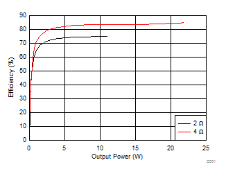
TSD5402-Q1 Output
            Power Efficiency Output Power Efficiency