SLLSEJ1A March 2014 – March 2014 TUSB551
PRODUCTION DATA.
- 1 Features
- 2 Applications
- 3 Description
- 4 Simplified Schematic
- 5 Revision History
- 6 Terminal Configuration and Functions
-
7 Specifications
- 7.1 Absolute Maximum Ratings
- 7.2 Handling Ratings
- 7.3 Recommended Operating Conditions
- 7.4 Thermal Information
- 7.5 Power Supply Electrical Characteristics
- 7.6 DC Electrical Characteristics
- 7.7 AC Electrical Characteristics
- 7.8 Timing Requirements/Timing Diagrams
- 7.9 Switching Characteristics
- 7.10 Typical Characteristics
- 8 Detailed Description
- 9 Applications and Implementation
- 10Power Supply Recommendations
- 11Layout
- 12Device and Documentation Support
- 13Mechanical, Packaging, and Orderable Information
Package Options
Mechanical Data (Package|Pins)
- RWB|12
Thermal pad, mechanical data (Package|Pins)
Orderable Information
11 Layout
11.1 Layout Guidelines
- The 100nF capacitors on the TXP and SSTXN nets should be placed close to the USB connector (Type A, Type B, and so forth).
- The ESD and EMI protection devices (if used) should also be placed as close as possible to the USB connector.
- Place voltage regulators as far away as possible from the differential pairs.
- In general, the large bulk capacitors associated with each power rail should be placed as close as possible to the voltage regulators.
- It is recommended that small decoupling capacitors for the 1.8V power rail be placed close to the TUSB551 as shown below.
- The SuperSpeed differential pair traces for RXP/N and TXP/N must be designed with a characteristic impedance of 90Ω ±10%. The PCB stack-up and materials will determine the width and spacing needed for a characteristic impedance of 90Ω.
- The SuperSpeed differential pair traces should be routed parallel to each other as much as possible. It is recommended the traces be symmetrical.
- In order to minimize cross talk, it is recommended to keep high speed signals away from each other. Each pair should be separated by at least 5 times the signal trace width. Separating with ground will also help minimize cross talk.
- Route all differential pairs on the same layer adjacent to a solid ground plane.
- Do not route differential pairs over any plane split.
- Adding test points will cause impedance discontinuity and will therefore negatively impact signal performance. If test points are used, they should be placed in series and symmetrically. They must not be placed in a manner that causes stub on the differential pair.
- Avoid 90 degree turns in traces. The use of bends in differential traces should be kept to a minimum. When bends are used, the number of left and right bends should be as equal as possible and the angle of the bend should be ≥ 135 degrees. This will minimize any length mismatch caused by the bends and therefore minimize the impact bends have on EMI.
- Match the etch lengths of the differential pair traces. There should be less than 5 mils difference between a SS differential pair signal and its complement. The USB 2.0 differential pairs should not exceed 50 mils relative trace length difference.
- The etch lengths of the differential pair groups do not need to match (i.e. the length of the RXP/N pair to that of the TXP/N pair), but all trace lengths should be minimized.
- Minimize the use of vias in the differential pair paths as much as possible. If this is not practical, make sure that the same via type and placement are used for both signals in a pair. Any vias used should be placed as close as possible to the TUSB551 device.
- To ease routing, the polarity of the SS differential pairs can be swapped. This means that TXP can be routed to TXN or RXN can be routed to RXP.
- Do not place power fuses across the differential pair traces.
11.2 Layout Example
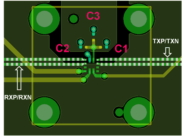 Figure 15. TUSB551 PCB Layout Example