SLLSEJ1A March 2014 – March 2014 TUSB551
PRODUCTION DATA.
- 1 Features
- 2 Applications
- 3 Description
- 4 Simplified Schematic
- 5 Revision History
- 6 Terminal Configuration and Functions
-
7 Specifications
- 7.1 Absolute Maximum Ratings
- 7.2 Handling Ratings
- 7.3 Recommended Operating Conditions
- 7.4 Thermal Information
- 7.5 Power Supply Electrical Characteristics
- 7.6 DC Electrical Characteristics
- 7.7 AC Electrical Characteristics
- 7.8 Timing Requirements/Timing Diagrams
- 7.9 Switching Characteristics
- 7.10 Typical Characteristics
- 8 Detailed Description
- 9 Applications and Implementation
- 10Power Supply Recommendations
- 11Layout
- 12Device and Documentation Support
- 13Mechanical, Packaging, and Orderable Information
Package Options
Mechanical Data (Package|Pins)
- RWB|12
Thermal pad, mechanical data (Package|Pins)
Orderable Information
6 Terminal Configuration and Functions
RWB Package
1.6 mm x 1.6 mm
(Top View)
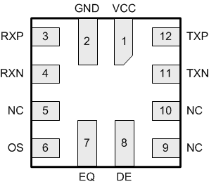
Terminal Functions
| TERMINAL | I/O | DESCRIPTION | |
|---|---|---|---|
| NAME | NO. | ||
| VCC | 1 | Power | 1.8 V Power Supply. |
| GND | 2 | GND | Ground. |
| RXP | 3 | Differential input | Differential input for 5Gbps SuperSpeed positive signals. |
| RXN | 4 | Differential input | Differential input for 5Gbps SuperSpeed negative signals. |
| NC | 5, 9, 10 | Not internally connected | |
| OS | 6 | CMOS Input | Sets output swing on the TX. 2-state input with integrated pull-up and pull-down resistors. |
| EQ | 7 | CMOS Input | Sets equalizer gain on the RX. 3-state input with integrated pull-up and pull-down resistors. |
| DE | 8 | CMOS Input | Sets output de-emphasis on the TX. 3-state input with integrated pull-up and pull-down resistors. |
| TXN | 11 | Differential output | Differential output for 5Gbps SuperSpeed negative signals. |
| TXP | 12 | Differential output | Differential output for 5Gbps SuperSpeed positive signals. |