SCES643I November 2006 – December 2024 TXB0108
ADVANCE INFORMATION
- 1
- 1 Features
- 2 Applications
- 3 Description
- 4 Pin Configuration and Functions
-
5 Specifications
- 5.1 Absolute Maximum Ratings
- 5.2 Handling Ratings
- 5.3 Recommended Operating Conditions
- 5.4 Thermal Information
- 5.5 Electrical Characteristics
- 5.6 Timing Requirements: VCCA = 1.2 V
- 5.7 Timing Requirements: VCCA = 1.5 V ± 0.1 V
- 5.8 Timing Requirements: VCCA = 1.8 V ± 0.15 V
- 5.9 Timing Requirements: VCCA = 2.5 V ± 0.2 V
- 5.10 Timing Requirements: VCCA = 3.3 V ± 0.3 V
- 5.11 Switching Characteristics: VCCA = 1.2 V
- 5.12 Switching Characteristics: VCCA = 1.5 V ± 0.1 V
- 5.13 Switching Characteristics: VCCA = 1.8 V ± 0.15 V
- 5.14 Switching Characteristics: VCCA = 2.5 V ± 0.2 V
- 5.15 Switching Characteristics: VCCA = 3.3 V ± 0.3 V
- 5.16 Operating Characteristics
- 5.17 Typical Characteristics
- 6 Parameter Measurement Information
- 7 Detailed Description
- 8 Application and Implementation
- 9 Power Supply Recommendations
- 10Layout
- 11Device and Documentation Support
- 12Revision History
- 13Mechanical, Packaging, and Orderable Information
Package Options
Refer to the PDF data sheet for device specific package drawings
Mechanical Data (Package|Pins)
- ZXY|20
- NME|20
- YZP|20
- DQS|20
- PW|20
- RGY|20
Thermal pad, mechanical data (Package|Pins)
Orderable Information
7.3.2 Input Driver Requirements
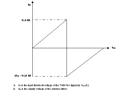
Typical IIN vs VIN characteristics of the TXB0108 are shown in Figure 7-2. For proper operation, the device driving the data I/Os of the TXB0108 must have drive strength of at least ±2 mA.
 Figure 7-2 Typical IIN vs VIN Curve