SCES643I November 2006 – December 2024 TXB0108
ADVANCE INFORMATION
- 1
- 1 Features
- 2 Applications
- 3 Description
- 4 Pin Configuration and Functions
-
5 Specifications
- 5.1 Absolute Maximum Ratings
- 5.2 Handling Ratings
- 5.3 Recommended Operating Conditions
- 5.4 Thermal Information
- 5.5 Electrical Characteristics
- 5.6 Timing Requirements: VCCA = 1.2 V
- 5.7 Timing Requirements: VCCA = 1.5 V ± 0.1 V
- 5.8 Timing Requirements: VCCA = 1.8 V ± 0.15 V
- 5.9 Timing Requirements: VCCA = 2.5 V ± 0.2 V
- 5.10 Timing Requirements: VCCA = 3.3 V ± 0.3 V
- 5.11 Switching Characteristics: VCCA = 1.2 V
- 5.12 Switching Characteristics: VCCA = 1.5 V ± 0.1 V
- 5.13 Switching Characteristics: VCCA = 1.8 V ± 0.15 V
- 5.14 Switching Characteristics: VCCA = 2.5 V ± 0.2 V
- 5.15 Switching Characteristics: VCCA = 3.3 V ± 0.3 V
- 5.16 Operating Characteristics
- 5.17 Typical Characteristics
- 6 Parameter Measurement Information
- 7 Detailed Description
- 8 Application and Implementation
- 9 Power Supply Recommendations
- 10Layout
- 11Device and Documentation Support
- 12Revision History
- 13Mechanical, Packaging, and Orderable Information
Package Options
Refer to the PDF data sheet for device specific package drawings
Mechanical Data (Package|Pins)
- ZXY|20
- NME|20
- YZP|20
- DQS|20
- PW|20
- RGY|20
Thermal pad, mechanical data (Package|Pins)
Orderable Information
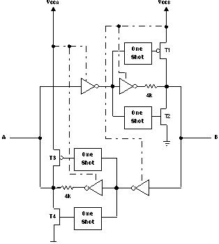
7.3.1 Architecture
The TXB0108 architecture (see Figure 7-1) does not require a direction-control signal to control the direction of data flow from A to B or from B to A. In a dc state, the output drivers of the TXB0108 can maintain a high or low, but are designed to be weak so that they can be overdriven by an external driver when data on the bus starts flowing the opposite direction. The output one-shots detect rising or falling edges on the A or B ports. During a rising edge, the one-shot turns on the PMOS transistors (T1, T3) for a short duration, which speeds up the low-to-high transition. Similarly, during a falling edge, the one-shot turns on the NMOS transistors (T2, T4) for a short duration, which speeds up the high-to-low transition. The typical output impedance during output transition is 70 Ω at VCCO = 1.2 V to 1.8 V, 50 Ω at VCCO = 1.8 V to 3.3 V and 40 Ω at VCCO = 3.3 V to 5 V.
 Figure 7-1 Architecture of TXB0108 I/O Cell