SCES638E October 2007 – December 2024 TXS0101
PRODUCTION DATA
- 1
- 1 Features
- 2 Applications
- 3 Description
- 4 Pin Configuration and Functions
-
5 Specifications
- 5.1 Absolute Maximum Ratings
- 5.2 ESD Ratings
- 5.3 Recommended Operating Conditions
- 5.4 Thermal Information
- 5.5 Electrical Characteristics
- 5.6 Switching Characteristics, VCCA = 1.8 ± 0.15 V
- 5.7 Switching Characteristics, VCCA = 2.5 ± 0.2 V
- 5.8 Switching Characteristics, VCCA = 3.3 ± 0.3 V
- 5.9 Switching Characteristics: Tsk, TMAX
- 5.10 Typical Characteristics
- 6 Parameter Measurement Information
- 7 Detailed Description
- 8 Application and Implementation
- 9 Device and Documentation Support
- 10Revision History
- 11Mechanical, Packaging, and Orderable Information
Package Options
Mechanical Data (Package|Pins)
Thermal pad, mechanical data (Package|Pins)
Orderable Information
3 Description
This one-bit non-inverting translator uses two separate configurable power-supply rails. The A port is designed to track VCCA. VCCA accepts any supply voltage from 1.65V to 3.6V. VCCA must be less than or equal to VCCB . The B port is designed to track VCCB. VCCB accepts any supply voltage from 2.3V to 5.5V. This allows for low voltage bidirectional translation between any of the 1.8V, 2.5V, 3.3V, and 5V voltage nodes.
When the output-enable (OE) input is low, all outputs are placed in the high-impedance state.
To put the device in the high-impedance state during power up or power down, tie OE to GND through a pull-down resistor; the current-sourcing capability of the driver determines the minimum value of the resistor.
| PART NUMBER | PACKAGE (1) | PACKAGE SIZE (2) |
|---|---|---|
| TXS0101 | DBV (SOT-23, 6) | 2.9mm × 2.8mm |
| DCK (SC70, 6) | 2mm × 2.1mm | |
| DRL (SOT-5X3, 6) | 1.6mm × 1.6mm | |
| DRY (SON, 6) | 1.45mm x 1mm |
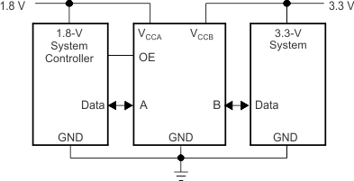
 Typical Operating Circuit