SCES638E October 2007 – December 2024 TXS0101
PRODUCTION DATA
- 1
- 1 Features
- 2 Applications
- 3 Description
- 4 Pin Configuration and Functions
-
5 Specifications
- 5.1 Absolute Maximum Ratings
- 5.2 ESD Ratings
- 5.3 Recommended Operating Conditions
- 5.4 Thermal Information
- 5.5 Electrical Characteristics
- 5.6 Switching Characteristics, VCCA = 1.8 ± 0.15 V
- 5.7 Switching Characteristics, VCCA = 2.5 ± 0.2 V
- 5.8 Switching Characteristics, VCCA = 3.3 ± 0.3 V
- 5.9 Switching Characteristics: Tsk, TMAX
- 5.10 Typical Characteristics
- 6 Parameter Measurement Information
- 7 Detailed Description
- 8 Application and Implementation
- 9 Device and Documentation Support
- 10Revision History
- 11Mechanical, Packaging, and Orderable Information
Package Options
Mechanical Data (Package|Pins)
Thermal pad, mechanical data (Package|Pins)
Orderable Information
4 Pin Configuration and Functions
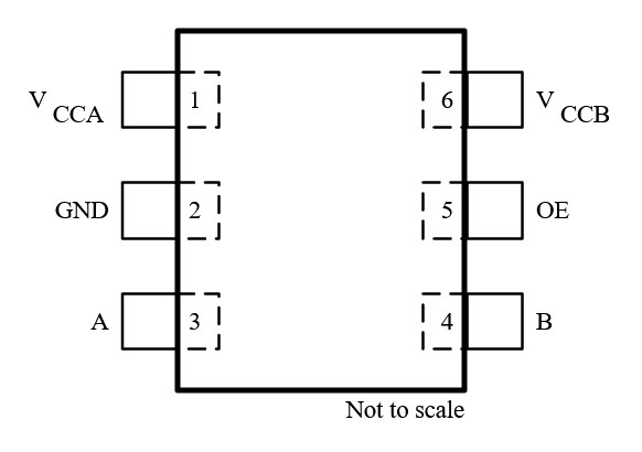
 Figure 4-1 DRY Package
 Figure 4-2 DBV, DCK, and DRL Package
Table 4-1 Pin Functions
| PIN | TYPE(1) | DESCRIPTION | |
|---|---|---|---|
| NAME | DBV, DCK, DRL, DRY | ||
| A | 3 | I/O | Input/output A. Referenced to VCCA |
| B | 4 | I/O | Input/output B. Referenced to VCCB |
| GND | 2 | G | Ground |
| OE | 5 | I | Output enable. Pull OE low to place all outputs in 3-state mode. Referenced to VCCA. |
| VCCA | 1 | I | A-port supply voltage. 1.65V ≤ VCCA ≤ 3.6V and VCCA ≤ VCCB |
| VCCB | 6 | I | B-port supply voltage. 2.3V ≤ VCCB ≤ 5.5V |
(1) I = input, O = output, G = ground