SCES964 June 2024 TXS0104V
PRODUCTION DATA
- 1
- 1 Features
- 2 Applications
- 3 Description
- 4 Pin Configuration and Functions
-
5 Specifications
- 5.1 Absolute Maximum Ratings
- 5.2 ESD Ratings
- 5.3 Recommended Operating Conditions
- 5.4 Thermal Information (PW, RGY, BQA, RUT, D)
- 5.5 Electrical Characteristics
- 5.6 Switching Characteristics, VCCA = 1.8 ± 0.15V
- 5.7 Switching Characteristics, VCCA = 2.5 ± 0.2V
- 5.8 Switching Characteristics, VCCA = 3.3 ± 0.3V
- 5.9 Switching Characteristics: Tsk, TMAX
- 5.10 Typical Characteristics
- 6 Parameter Measurement Information
- 7 Detailed Description
- 8 Application and Implementation
- 9 Device and Documentation Support
- 10Revision History
- 11Mechanical, Packaging, and Orderable Information
Package Options
Mechanical Data (Package|Pins)
Thermal pad, mechanical data (Package|Pins)
- BQA|14
Orderable Information
5.10 Typical Characteristics

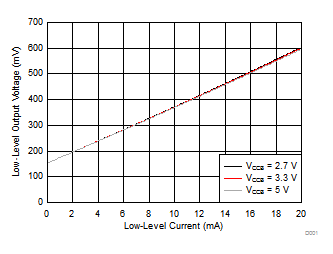
| VCCA = 1.8 V | VIL(A) = 150 mV |
vs Low-Level Current (IOL(Ax))

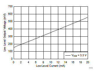
| VCCA = 3.3 V | VIL(A) = 150 mV |

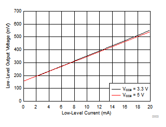
| VCCA = 2.7 V | VIL(A) = 150 mV |
vs Low-Level Current (IOL(Ax))