SGLS384B May 2008 – October 2024 UC2843A-Q1
PRODUCTION DATA
- 1
- 1 Features
- 2 Applications
- 3 Description
- 4 Pin Configuration and Functions
- 5 Specifications
- 6 Detailed Description
- 7 Application and Implementation
- 8 Power Supply Recommendations
- 9 Layout
- 10Device and Documentation Support
- 11Revision History
- 12Mechanical, Packaging, and Orderable Information
Package Options
Mechanical Data (Package|Pins)
- D|8
Thermal pad, mechanical data (Package|Pins)
Orderable Information
7.2 Typical Application
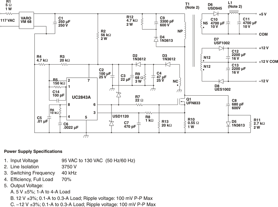
A typical application for the UC2843A-Q1 in an off-line flyback converter is shown in Figure 7-1. The UC2843A uses an inner current control loop that contains a small current sense resistor which senses the primary inductor current ramp. This current sense resistor transforms the inductor current waveform to a voltage signal that is input directly into the primary side PWM comparator. This inner loop determines the response to input voltage changes. An outer voltage control loop involves comparing a portion of the output voltage to a reference voltage at the input of an error amplifier. When used in an off-line isolated application, the voltage feedback of the isolated output is accomplished using a secondary-side error amplifier and adjustable voltage reference, such as the TL431. The error signal crosses the primary to secondary isolation boundary using an opto-isolator whose collector is connected to the VREF pin and the emitter is connected to FB. The outer voltage control loop determines the response to load changes.
 Figure 7-1 Typical
Flyback Application Circuit