SGLS384B May 2008 – October 2024 UC2843A-Q1
PRODUCTION DATA
- 1
- 1 Features
- 2 Applications
- 3 Description
- 4 Pin Configuration and Functions
- 5 Specifications
- 6 Detailed Description
- 7 Application and Implementation
- 8 Power Supply Recommendations
- 9 Layout
- 10Device and Documentation Support
- 11Revision History
- 12Mechanical, Packaging, and Orderable Information
Package Options
Mechanical Data (Package|Pins)
- D|8
Thermal pad, mechanical data (Package|Pins)
Orderable Information
6.3.5 Oscillator
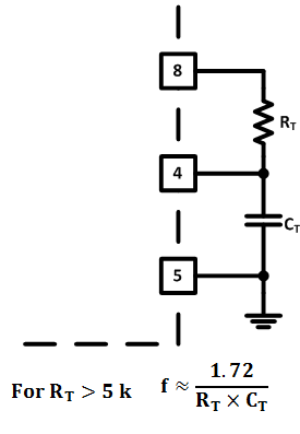
 Figure 6-4 Oscillator Frequency vs Timing Resistance
 Figure 6-5 Maximum Duty Cycle vs Timing Resistance
 Figure 6-6 Oscillator Section
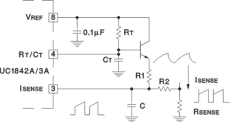
 Figure 6-7 Slope Compensation
Precision operation at high frequencies with an accurate maximum duty cycle, see Figure 6-5, can now be obtained with the UC2843A-Q1 device due to its trimmed oscillator discharge current. This nullifies the effects of production variations in the initial discharge current or dead time.
A fraction of the oscillator ramp can be resistively summed with the current sense signal, to provide slope compensation for converters requiring duty cycles over 50%. Capacitor C forms a filter with R2 to suppress the leading-edge switch spikes.