SGLS164A April 2003 – October 2024 UC2842AQ , UC2843AQ , UC2844AQ , UC2845AQ
PRODUCTION DATA
- 1
- 1 Features
- 2 Applications
- 3 Description
- 4 Pin Configuration and Functions
- 5 Specifications
- 6 Parameter Measurement Information
- 7 Detailed Description
- 8 Application and Implementation
- 9 Device and Documentation Support
- 10Revision History
- 11Mechanical, Packaging, and Orderable Information
Package Options
Refer to the PDF data sheet for device specific package drawings
Mechanical Data (Package|Pins)
- D|8
- D|14
Thermal pad, mechanical data (Package|Pins)
Orderable Information
4 Pin Configuration and Functions
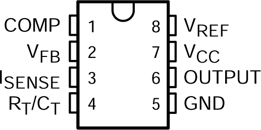
 Figure 4-1 D 8-Pin Package (Top View)
| PIN | TYPE(1) | DESCRIPTION | |
|---|---|---|---|
| NAME | NO. | ||
| COMP | 1 | O | Outputs the low impedance 1-MHz internal error amplifier that is also the input to the peak current limit or PWM comparator, with an open-loop gain (AVOL) of 90 dB. This pin is capable of sinking a maximum of 6 mA and is not internally current limited. |
| VFB | 2 | I | Input to the error amplifier that can be used to control the power converter voltage feedback loop for stability |
| ISENSE | 3 | I | Input to the peak current limit, PWM comparator of the controllers. When used in conjunction with a current sense resistor, the error amplifier output voltage controls the power systems cycle-by-cycle peak current limit. The maximum peak current sense signal is internally clamped to 1 V. See the Functional Block Diagram |
| RT/CT | 4 | I | Input to the internal oscillator that is programmed with an external timing resistor (RT) and timing capacitor (CT). See Oscillator for information on properly selecting these timing components. TI recommends using capacitance values from 470 pF to 4.7 nF. TI also recommends that the timing resistor values chosen be from 5 kΩ to 100 kΩ. |
| GND | 5 | GND | Controller signal ground. |
| OUTPUT | 6 | O | Output of 1-A totem pole gate driver. This pin can sink and source up to 1 A of gate driver current. A gate driver resistor must be used to limit the gate driver current. |
| VCC | 7 | I |
Analog controller bias input that provides power to the device. Total VCC current is the sum of the quiescent VCC current and the average OUTPUT current. Knowing the switching frequency and the MOSFET gate charge, Qg, the average OUTPUT current can be calculated from: IOUTPUT = Qg × fSW A bypass capacitor, typically 0.1 µF, connected directly to GROUND with minimal trace length, is required on this pin. An additional bypass capacitor at least 10 times greater than the gate capacitance of the main switching FET used in the design is also required on VCC. |
| VREF | 8 | O | Bias input to the gate driver. This pin must have a biasing capacitor that is at least 10 times greater than the gate capacitance of the main switching FET used in the design. |
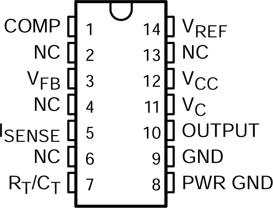
 Figure 4-2 D 14-Pin Package (Top View)
| PIN | TYPE(1) | DESCRIPTION | |
|---|---|---|---|
| NAME | NO. | ||
| COMP | 1 | I/O | Error amplifier compensation pin |
| NC | 2 | - | Do not connect |
| VFB | 3 | I | Error amplifier input |
| NC | 4 | - | Do not connect |
| ISENSE | 5 | I | Current sense comparator input |
| NC | 6 | - | Do not connect |
| RT/CT | 7 | I/O | Oscillator RC input |
| PWR GND | 8 | GND | Output PWM ground terminal |
| GND | 9 | GND | Device power supply ground terminal |
| OUTPUT | 10 | O | PWM Output |
| VS | 11 | - | Output PWM positive voltage supply |
| VCC | 12 | - | Device positive voltage supply |
| NC | 13 | - | Do not connect |
| VREF | 14 | O | Oscillator voltage reference |