SGLS164A April 2003 – October 2024 UC2842AQ , UC2843AQ , UC2845AQ
PRODUCTION DATA
- 1
- 1 Features
- 2 Applications
- 3 Description
- 4 Pin Configuration and Functions
- 5 Specifications
- 6 Parameter Measurement Information
- 7 Detailed Description
- 8 Application and Implementation
- 9 Device and Documentation Support
- 10Revision History
- 11Mechanical, Packaging, and Orderable Information
Package Options
Refer to the PDF data sheet for device specific package drawings
Mechanical Data (Package|Pins)
- D|8
- D|14
Thermal pad, mechanical data (Package|Pins)
Orderable Information
8.1 Application Information
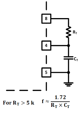
 Figure 8-1 Oscillator
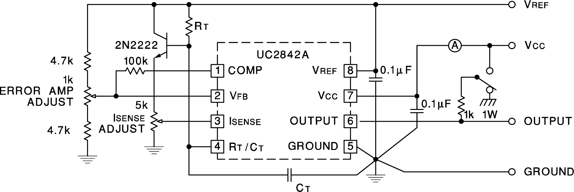
 Figure 8-2 Open-Loop Laboratory Text
Fixture
Figure 8-2 Open-Loop Laboratory Text
FixtureHigh peak currents associated with capacitive loads necessitate careful grounding techniques. Timing and bypass capacitors must be connected close to pin 5 in a single point ground. The transistor and 5k potentiometer are used to sample the oscillator waveform and apply an adjustable ramp to pin 3.
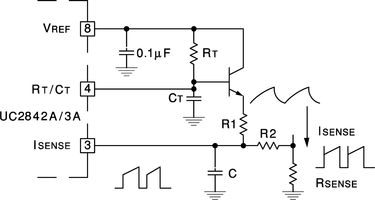
 Figure 8-3 Slope Compression
A fraction of the oscillator ramp can be resistively summed with the current sense signal to provide slope compensation for converters requiring duty cycles over 50%. Note that capacitor, C, forms a filter with R2 to suppress the leading edge switch spikes.
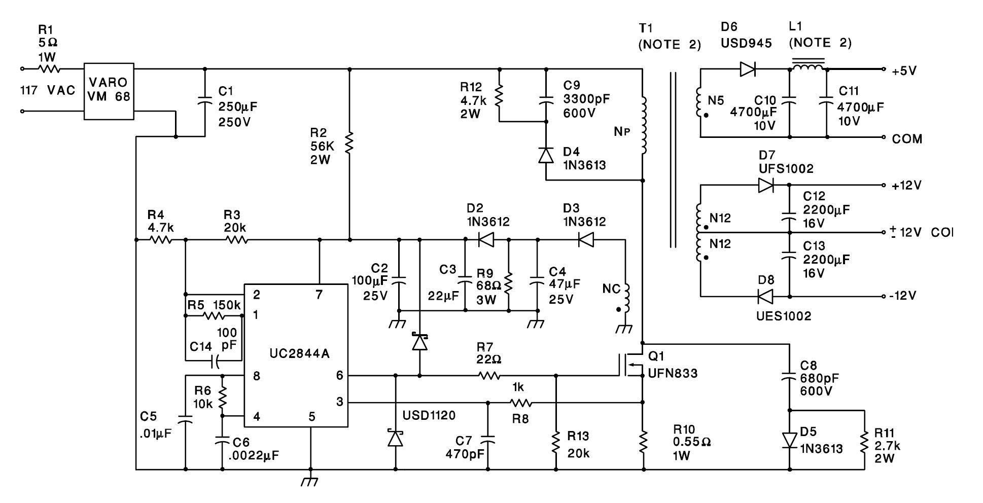
 Figure 8-4 Off-Line Flyback
Regulator
- Input Voltage: 95 VAC to 130 VAC (50Hz/60Hz)
- Line Isolation: 3750V
- Switching Frequency 40 kHz
- Efficiency, Full Load: 70%
- Output Voltage:
- +5V, ±5%; 1A to 4A Load
- +12V, ±3%; 0.1A to 0.3A Load Ripple voltage: 100 mV P-P Max
- –12V, ±3%; 0.1A to 0.3A Load Ripple voltage: 100 mV P-P Max