SNVSBY2A January 2021 – June 2021 UCC12051-Q1
PRODUCTION DATA
- 1 Features
- 2 Applications
- 3 Description
- 4 Revision History
- 5 Pin Configuration and Functions
-
6 Specifications
- 6.1 Absolute Maximum Ratings
- 6.2 ESD Ratings
- 6.3 Recommended Operating Conditions
- 6.4 Thermal Information
- 6.5 Power Ratings
- 6.6 Insulation Specifications
- 6.7 Safety-Related Certifications
- 6.8 Safety Limiting Values
- 6.9 Electrical Characteristics
- 6.10 Switching Characteristics
- 6.11 Insulation Characteristics Curves
- 6.12 Typical Characteristics
- 7 Detailed Description
- 8 Application and Implementation
- 9 Power Supply Recommendations
- 10Layout
- 11Device and Documentation Support
- 12Mechanical, Packaging, and Orderable Information
Package Options
Mechanical Data (Package|Pins)
- DVE|16
Thermal pad, mechanical data (Package|Pins)
Orderable Information
7.3.3 VISO Load Recommended Operating Area
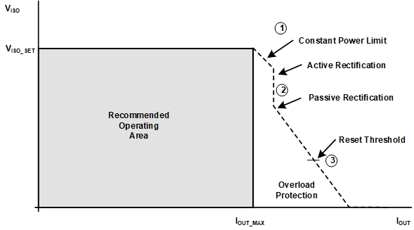
Figure 7-1 depicts the device VISO regulation behavior across the output load range, including when the output is overloaded. For proper device operation, ensure that the device VISO output load does not exceed the maximum output current (IOUT_MAX). The value for IOUT_MAX over different temperature and VINP conditions are shown from Figure 6-8 to Figure 6-11. The following protection mechanisms will be engaged if the UCC12051-Q1 is loaded beyond the recommended operating area:
- The device limits the maximum output power. If a load exceeding IOUT_MAX is applied, VISO drops accordingly to meet the maximum power limit.
- If VISO drops below nominal 3.8 V while operating in the constant power limit region, the over-power fold-back feature will switch the power converter from active rectification to passive rectification, and the built-in recovery hysteresis will ensure the UCC12051-Q1 recovers at a lower output power. The device returns to active rectification when load drops and VISO increases above nominal 4.3 V.
- The device triggers a soft-start reset if VISO drops below the nominal 1.8-V threshold. This reset is designed to protect the device during VISO short-circuit conditions.
- Thermal shutdown protection disables the converter if the device is operated in any of the above regions long enough to raise the silicon junction temperature above the thermal shutdown threshold. See the Section 7.3.4 section for more details on this device feature.
 Figure 7-1 VISO Load Recommended Operating Area Description