SLUSDO2D June 2020 – August 2024 UCC21540-Q1
PRODUCTION DATA
- 1
- 1 Features
- 2 Applications
- 3 Description
- 4 Device Comparison Table
- 5 Pin Configuration and Functions
-
6 Specifications
- 6.1 Absolute Maximum Ratings
- 6.2 ESD Ratings
- 6.3 Recommended Operating Conditions
- 6.4 Thermal Information
- 6.5 Power Ratings
- 6.6 Insulation Specifications
- 6.7 Safety-Limiting Values
- 6.8 Electrical Characteristics
- 6.9 Switching Characteristics
- 6.10 Insulation Characteristics Curves
- 6.11 Typical Characteristics
- 7 Parameter Measurement Information
- 8 Detailed Description
-
9 Application and Implementation
- 9.1 Application Information
- 9.2
Typical Application
- 9.2.1 Design Requirements
- 9.2.2
Detailed Design Procedure
- 9.2.2.1 Designing INA/INB Input Filter
- 9.2.2.2 Select Dead Time Resistor and Capacitor
- 9.2.2.3 Select External Bootstrap Diode and Its Series Resistor
- 9.2.2.4 Gate Driver Output Resistor
- 9.2.2.5 Gate to Source Resistor Selection
- 9.2.2.6 Estimating Gate Driver Power Loss
- 9.2.2.7 Estimating Junction Temperature
- 9.2.2.8 Selecting VCCI, VDDA/B Capacitor
- 9.2.2.9 Application Circuits with Output Stage Negative Bias
- 9.2.3 Application Curves
- 10Power Supply Recommendations
- 11Layout
- 12Device and Documentation Support
- 13Revision History
- 14Mechanical, Packaging, and Orderable Information
Package Options
Refer to the PDF data sheet for device specific package drawings
Mechanical Data (Package|Pins)
- DWK|14
Thermal pad, mechanical data (Package|Pins)
Orderable Information
7.6 Power-Up UVLO Delay to OUTPUT
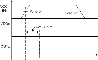
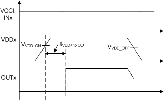
Whenever the supply voltage VCCI crosses from below the falling threshold VVCCI_OFF to above the rising threshold VVCCI_ON, and whenever the supply voltage VDDx crosses from below the falling threshold VVDDx_OFF to above the rising threshold VVDDx_ON, there is a delay before the outputs begin responding to the inputs. For VCCI UVLO this delay is defined as tVCCI+ to OUT, and has a maximum value of 50 µs. For VDDx UVLO this delay is defined as tVDD+ to OUT, and has a maximum value of 10 µs. TI recommends allowing some margin before driving input signals, to ensure the driver VCCI and VDD bias supplies are fully activated. Figure 7-7 and Figure 7-8 show the power-up UVLO delay timing diagram for VCCI and VDD.
Whenever the supply voltage VCCI crosses below the falling threshold VVCCI_OFF, or VDDx crosses below the falling threshold VVDDx_OFF, the outputs stop responding to the inputs and are held low within ≤2 µs. This asymmetric delay is designed to ensure safe operation during VCCI or VDDx brownouts.
When VCCI goes away but VDDx is present, outputs are held low; when VDDx is gone, outputs are CLAMPED low through the active pull down feature. For more detailed UVLO feature description, please check session Section 8.3.1.
 Figure 7-7 VCCI Power-up UVLO Delay
 Figure 7-8 VDDA/B
Power-Up
UVLO Delay