SLUSEU6D May 2023 – August 2024 UCC21550-Q1
PRODUCTION DATA
- 1
- 1 Features
- 2 Applications
- 3 Description
- 4 Pin Configuration and Functions
-
5 Specifications
- 5.1 Absolute Maximum Ratings
- 5.2 ESD Ratings (Automotive)
- 5.3 Recommended Operating Conditions
- 5.4 Thermal Information
- 5.5 Power Ratings
- 5.6 Insulation Specifications
- 5.7 Safety Limiting Values
- 5.8 Electrical Characteristics
- 5.9 Switching Characteristics
- 5.10 Insulation Characteristics Curves
- 5.11 Typical Characteristics
- 6 Parameter Measurement Information
- 7 Detailed Description
-
8 Application and Implementation
- 8.1 Application Information
- 8.2
Typical Application
- 8.2.1 Design Requirements
- 8.2.2
Detailed Design Procedure
- 8.2.2.1 Designing INA/INB Input Filter
- 8.2.2.2 Select External Bootstrap Diode and its Series Resistor
- 8.2.2.3 Gate Driver Output Resistor
- 8.2.2.4 Gate to Source Resistor Selection
- 8.2.2.5 Estimate Gate Driver Power Loss
- 8.2.2.6 Estimating Junction Temperature
- 8.2.2.7 Selecting VCCI, VDDA/B Capacitor
- 8.2.2.8 Dead Time Setting Guidelines
- 8.2.2.9 Application Circuits with Output Stage Negative Bias
- 8.2.3 Application Curves
- 9 Power Supply Recommendations
- 10Layout
- 11Device and Documentation Support
- 12Revision History
- 13Mechanical, Packaging, and Orderable Information
Package Options
Refer to the PDF data sheet for device specific package drawings
Mechanical Data (Package|Pins)
- DWK|14
- DW|16
Thermal pad, mechanical data (Package|Pins)
Orderable Information
3 Description
The UCC21550-Q1 is an isolated dual channel gate driver family with programmable dead time and wide temperature range. It is designed with 4A peak-source and 6A peak-sink current to drive power MOSFET, SiC, GaN, and IGBT transistors.
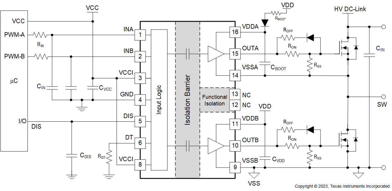
The UCC21550-Q1 can be configured as two low-side drivers, two high-side drivers, or a half-bridge driver. The input side is isolated from the two output drivers by a 5kVRMS isolation barrier, with a minimum of 125V/ns common-mode transient immunity (CMTI).
Protection features include: resistor programmable dead time, disable feature to shut down both outputs simultaneously, and integrated de-glitch filter that rejects input transients shorter than 5ns. All supplies have UVLO protection.
With all these advanced features, the UCC21550-Q1 device enables high efficiency, high power density, and robustness in a wide variety of power applications.
| PART NUMBER | PACKAGE(1) | REC. VDD SUPPLY MIN |
|---|---|---|
| UCC21550AQDWRQ1 | DW (SOIC, 16) | 6.5V |
| UCC21550BQDWRQ1 | DW (SOIC, 16) | 9.2V |
| UCC21550AQDWKRQ1 | DWK (SOIC, 14) | 6.5V |
| UCC21550BQDWKRQ1 | DWK (SOIC, 14) | 9.2V |
| UCC21550CQDWKRQ1 | DWK (SOIC, 14) | 13.5V |
 Typical Application Schematic