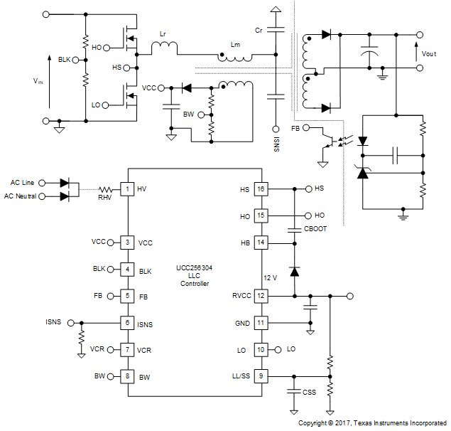
The UCC256304 is a fully featured LLC controller with integrated high-voltage gate driver. It has been designed to pair with a PFC stage to provide a complete power system using a minimum of external components. The resulting power system is designed to meet the most stringent requirements for standby power without the need for a separate standby power converter.UCC256304 uses hybrid hysteretic control to provide best in class line and load transient response. The control makes the open loop transfer function a first order system so that it’s very easy to compensate and is always stable with proper frequency compensation.
The UCC256304 is unique in that the controller is able to operate over a large DC input range. This is accomplished by making the input overvoltage sense threshold much larger than the input voltage start threshold. This allows the LLC to startup and enter a low power standby mode without the need to enable the PFC and enables the LLC to accommodate an extensive range of common AC inputs.
UCC256304 provides a highly efficient burst mode with consistent burst power level during each burst on cycle. The burst power level is programmable and adaptively changes with input voltage.
PART NUMBER | PACKAGE | BODY SIZE (NOM) |
---|---|---|
UCC256304 | SOIC (14) | 9.9 mm x 3.9 mm |
DATE | REVISION | NOTES |
---|---|---|
October 2017 | * | Initial release. |
PIN | I/O | DESCRIPTION | |
---|---|---|---|
NAME | NO. | ||
BLK | 4 | I | This pin is used to sense the PFC output voltage level. A resistive divider should be used to attenuate the signal before it is applied to this pin. The voltage level on this pin will determine when the LLC converter start/stops switching. The sensed BLK voltage is also used to adjust the burst mode threshold to improve efficiency over the input voltage range. |
BW | 8 | I | This pin is used to sense the output voltage through the bias winding. The sensed voltage is used for output over voltage protection. |
FB | 5 | I | LLC stage control feedback input. The amount of current sourced from this pin will determine the LLC input power level. |
GND | 11 | G | Ground reference for all signals. |
HB | 14 | I | High-side gate-drive floating supply voltage. The bootstrap capacitor is connected between this pin and pin HS. A high voltage, high speed diode should be connected from RVCC to this pin to supply power to the upper MOSFET driver during the period when the lower MOSFET is conducting. |
HO | 15 | O | High-side floating gate-drive output. |
HS | 16 | I | High-side gate-drive floating ground. Current return for the high-side gate-drive current. |
HV | 1 | I | Connects to Internal HV startup JFET. This pin provides start up power for both PFC and LLC stage. This pin also monitors the AC line voltage for x-capacitor discharge function. |
ISNS | 6 | I | Resonant current sense. The resonant capacitor voltage is differentiated with a first order filter to measure the resonant current |
LL/SS | 9 | I | The capacitance value connected from this pin to ground will define the duration of the soft-start period. This pin is also used to program the burst mode threshold; the resistor divider on this pin programs the burst mode threshold and the threshold scaling factor with BLK pin voltage. |
LO | 10 | O | Low-side gate-drive output. |
Missing | 2 | N/A | Functional creepage and clearance |
Missing | 13 | N/A | Functional creepage and clearance |
RVCC | 12 | P | Regulated 12-V supply. This pin is used to supply the gate driver and PFC controller. |
VCC | 3 | P | Supply input. |
VCR | 7 | I | Resonant capacitor voltage sense |
MIN | MAX | UNIT | ||
---|---|---|---|---|
Input voltage | HV, HB | –0.3 | 640 | V |
BLK, FB, LL/SS | –0.3 | 7 | V | |
VCR | –0.3 | 7 | V | |
HB - HS | –0.3 | 17 | V | |
VCC | –0.3 | 30 | V | |
BW, ISNS | –5 | 7 | V | |
RVCC output voltage | DC | –0.3 | 17 | V |
HO output voltage | DC | HS – 0.3 | HB + 0.3 | V |
Transient, less than 100ns | HS – 2 | HB + 0.3 | ||
LO output voltage | DC | –0.3 | RVCC + 0.3 | V |
Transient, less than 100ns | –2 | RVCC + 0.3 | ||
Floating ground slew rate | dVHS/dt | –50 | 50 | V/ns |
HO, LO pulsed current | IOUT_PULSED | –0.6 | 1.2 | A |
Junction temperature range | TJ | –40 | 150 | °C |
Storage temperature range, Tstg | Tstg | –65 | 150 | |
Lead temperature | Soldering, 10 second | 300 | ||
Reflow | 260 |
VALUE | UNIT | |||
---|---|---|---|---|
V(ESD) | Electrostatic discharge | Human body model (HBM), per ANSI/ESDA/JEDEC JS-001, high voltage pins(1) | ±1000 | V |
Human body model (HBM), per ANSI/ESDA/JEDEC JS-001, all other pins(1) | ±2000 | |||
Charged device model (CDM), per JEDEC specification JESD22-C101, all pins(2) | ±500 |
MIN | NOM | MAX | UNIT | ||
---|---|---|---|---|---|
HV, HS | Input voltage | 600 | V | ||
VCC | Supply voltage | 13 | 15 | 26 | V |
HB - HS | Driver bootstrap voltage | 10 | 12 | 16 | V |
CB | Ceramic bypass capacitor from HB to HS | 0.1 | 5 | µF | |
CRVCC | RVCC pin decoupling capacitor | 4.7 | µF | ||
IRVCCMAX | Maximum output current of RVCC (1) | 100 | mA | ||
TA | Operating ambient temperature | -40 | 125 | °C |
THERMAL METRIC(1) | UCC256304 | UNIT | |
---|---|---|---|
D (SOIC) | |||
14 PINS | |||
RθJA | Junction-to-ambient thermal resistance | 74.7 | °C/W |
RθJC(top) | Junction-to-case (top) thermal resistance | 30.7 | °C/W |
RθJB | Junction-to-board thermal resistance | 31.8 | °C/W |
ΨJT | Junction-to-top characterization parameter | 4.4 | °C/W |
ΨJB | Junction-to-board characterization parameter | 31.4 | °C/W |
PARAMETER | TEST CONDITIONS | MIN | TYP | MAX | UNIT | |
---|---|---|---|---|---|---|
SUPPLY VOLTAGE | ||||||
VCCShort | Below this threshold, use reduced start up current | 0.5 | 0.6 | 0.7 | V | |
VCCReStartJfet | Below this threshold, re-enable JFET. | 10.2 | 10.5 | 10.8 | V | |
VCCStartSelf | In self bias mode, gate starts switching above this level | 25 | 26 | 28 | V | |
SUPPLY CURRENT | ||||||
ICCSleep | Current drawn from VCC rail during burst off period | VCC = 15V | 475 | 565 | 700 | µA |
ICCRun | Current drawn from VCC Pin while gate is switching. Excluding Gate Current | VCC = 15V, maximum dead time | 1.75 | 2.2 | 2.65 | mA |
REGULATED SUPPLY | ||||||
VRVCC | Regulated supply voltage | VCC = 15V | 11.60 | 12 | 12.40 | V |
VCC = 13V | 11.2 | 11.8 | 12.25 | V | ||
VRVCCUVLO | RVCC under voltage lock out voltage (1) | 7 | V | |||
HIGH VOLTAGE STARTUP | ||||||
IHVLow | Reduced startup pin current | 0.28 | 0.41 | 0.54 | mA | |
IHVHigh | Full startup pin current | 7.6 | 10.20 | 12.6 | mA | |
IHVLeak | HV current source leakage current | 1.40 | 3.37 | 7.55 | µA | |
IHVZCD | Highest AC zero crossing detection test current | 0.63 | 0.77 | 0.89 | mA | |
IXCAPDischarge | X-cap discharge current | 9.6 | 11.47 | 13.5 | mA | |
tXCAPZCD | AC zero crossing detection window length for first three test current stage (1) | 10 | 11.85 | 14 | ms | |
tXCAPZCDLast | AC zero crossing detection window length for final test current stage (1) | 43 | 46 | 52 | ms | |
tXCAPIdle | AC zero crossing detection idle period length (1) | 635 | 704 | 772 | ms | |
tXCAPDischarge | Time for X-cap discharge current active (1) | 327 | 358 | 390 | ms | |
BULK VOLTAGE SENSE | ||||||
VBLKStart | Input voltage that allows LLC to start switching | Voltage rising | 1.01 | 1.04 | 1.08 | V |
VBLKStop | Input voltage that forces LLC operation to stop | Voltage falling | 0.83 | 0.87 | 0.93 | V |
VBLKOVRise | Input voltage that causes switching to stop | Voltage rising | 4.92 | 5.03 | 5.12 | V |
VBLKOVFall | Input voltage that causes switching to re-start | Voltage falling | 3.67 | 3.76 | 3.86 | V |
FEEDBACK PIN | ||||||
RFBInternal | Internal pull down resistor value | 90.7 | 101.5 | 112.3 | kΩ | |
IFB | FB internal current source | 76.5 | 85.1 | 93.6 | µA | |
f-3dB | Feedback chain -3dB cut off frequency (2) | 1 | MHz | |||
RESONANT CURRENT SENSE | ||||||
VISNS_OCP1 | OCP1 threshold | 3.97 | 4.03 | 4.07 | V | |
VISNS_OCP1_SS | OCP1 threshold during soft start (1) | 5 | V | |||
VISNS_OCP2 | OCP2 threshold | 0.68 | 0.84 | 0.99 | V | |
VISNS_OCP3 | OCP3 threshold | 0.49 | 0.64 | 0.79 | V | |
TISNS_OCP2 | The time the average input current needs to stay above OCP2 threshold before OCP2 is triggered (1) | 2 | ms | |||
TISNS_OCP3 | The time the average input current needs to stay above OCP3 threshold before OCP3 is triggered (1) | 50 | ms | |||
VIpolarityHyst | Resonant current polarity detection hysteresis | 16.9 | 30.7 | 44.7 | mV | |
nOCP1 | Number of OCP1 cycles before OCP1 fault is tripped (1) | 4 | ||||
RESONANT CAPACITOR VOLTAGE SENSE | ||||||
VCM | Internal common mode voltage | 2.91 | 3.02 | 3.14 | V | |
IRAMP | Frequency compensation ramp current source value | 1.63 | 1.84 | 2.10 | mA | |
IMismatch | Pull up and pull down ramp current source mismatch (3) | -1.25 | 1.25 | % | ||
SOFT START | ||||||
ISSUp | Current output from SS pin to charge up the soft start capacitor | 21.8 | 25.8 | 29.8 | µA | |
RSSDown | SS pin pull down resistance |
ZCS or OCP1 | 222 | 401 | 580 | Ω |
GATE DRIVER | ||||||
VLOL | LO output low voltage | Isink = 20 mA | 0.027 | 0.052 | 0.087 | V |
VRVCC - VLOH | LO output high voltage | Isource = 20 mA | 0.113 | 0.178 | 0.263 | V |
VHOL - VHS | HO output low voltage | Isink = 20 mA | 0.027 | 0.053 | 0.087 | V |
VHB - VHOH | HO output high voltage | Isource = 20 mA | 0.113 | 0.173 | 0.263 | V |
VHB-HSUVLORise | High side gate driver UVLO rise threshold | 7.35 | 7.94 | 8.70 | V | |
VHB-HSUVLOFall | High side gate driver UVLO fall threshold | 6.65 | 7.25 | 7.76 | V | |
Isource_pk | HO, LO peak source current (2) | -0.6 | A | |||
Isink_pk | HO, LO peak sink current (2) | 1.2 | A | |||
BOOTSTRAP | ||||||
IBOOT_QUIESCENT | (HB - HS) quiescent current | HB - HS = 12 V | 51.10 | 74.40 | 97.70 | µA |
IBOOT_LEAK | HB to GND leakage current | 0.02 | 0.40 | 5.40 | µA | |
tChargeBoot | Length of charge boot state | 234 | 267 | 296 | µs | |
BIAS WINDING | ||||||
VBWOVRise | Output voltage OVP | -4.1 | -3.97 | -3.86 | V | |
BURST MODE | ||||||
RLL | LL voltage scaling resistor value | 240 | 250 | 258 | kΩ | |
ADAPTIVE DEADTIME | ||||||
dVHS/dt | Detectable PSN slew rate (1) | ±1 | ±50 | V/ns | ||
FAULT RECOVERY | ||||||
tPauseTimeOut | Paused timer (1) | 1 | s | |||
THERMAL SHUTDOWN | ||||||
TJ_r | Thermal shutdown temperature (1) | Temperature rising | 125 | 145 | °C | |
TJ_H | Thermal shutdown hsyterisis (1) | 20 | °C |
PARAMETER | TEST CONDITIONS | MIN | TYP | MAX | UNIT | |
---|---|---|---|---|---|---|
tr(LO) | Rise time | 10% to 90%, 1-nF load | 18 | 35 | 50 | ns |
tf(LO) | Fall time | 10% to 90%, 1-nF load | 15 | 25 | 50 | ns |
tr(HO) | Rise time | 10% to 90%, 1-nF load | 18 | 35 | 50 | ns |
tf(HO) | Fall time | 10% to 90%, 1-nF load | 15 | 25 | 50 | ns |
tDT(min) | Minimum dead time (1) | 100 | ns | |||
tDT(max) | Maximum dead time (dead time fault) (1) | 150 | µs | |||
tON(min) | Minimum gate on time (1) | 250 | ns | |||
tON(max) | Maximum gate on time (1) | 14.5 | µs |