SLUSD60 October 2017 UCC256304
PRODUCTION DATA.
- 1 Features
- 2 Applications
- 3 Description
- 4 Revision History
- 5 Pin Configuration and Functions
- 6 Specifications
-
7 Detailed Description
- 7.1 Overview
- 7.2 Functional Block Diagram
- 7.3
Feature Description
- 7.3.1 Hybrid Hysteretic Control
- 7.3.2 Regulated 12-V Supply
- 7.3.3 Feedback Chain
- 7.3.4 Optocoupler Feedback Signal Input and Bias
- 7.3.5 System External Shut Down
- 7.3.6 Pick Lower Block and Soft Start Multiplexer
- 7.3.7 Pick Higher Block and Burst Mode Multiplexer
- 7.3.8 VCR Comparators
- 7.3.9 Resonant Capacitor Voltage Sensing
- 7.3.10 Resonant Current Sensing
- 7.3.11 Bulk Voltage Sensing
- 7.3.12 Output Voltage Sensing
- 7.3.13 High Voltage Gate Driver
- 7.3.14 Protections
- 7.4 Device Functional Modes
-
8 Application and Implementation
- 8.1 Application Information
- 8.2
Typical Application
- 8.2.1 Design Requirements
- 8.2.2
Detailed Design Procedure
- 8.2.2.1 Custom Design With WEBENCH® Tools
- 8.2.2.2 LLC Power Stage Requirements
- 8.2.2.3 LLC Gain Range
- 8.2.2.4 Select Ln and Qe
- 8.2.2.5 Determine Equivalent Load Resistance
- 8.2.2.6 Determine Component Parameters for LLC Resonant Circuit
- 8.2.2.7 LLC Primary-Side Currents
- 8.2.2.8 LLC Secondary-Side Currents
- 8.2.2.9 LLC Transformer
- 8.2.2.10 LLC Resonant Inductor
- 8.2.2.11 LLC Resonant Capacitor
- 8.2.2.12 LLC Primary-Side MOSFETs
- 8.2.2.13 Design Considerations for Adaptive Dead-Time
- 8.2.2.14 LLC Rectifier Diodes
- 8.2.2.15 LLC Output Capacitors
- 8.2.2.16 HV Pin Series Resistors
- 8.2.2.17 BLK Pin Voltage Divider
- 8.2.2.18 BW Pin Voltage Divider
- 8.2.2.19 ISNS Pin Differentiator
- 8.2.2.20 VCR Pin Capacitor Divider
- 8.2.2.21 Burst Mode Programming
- 8.2.2.22 Soft-Start Capacitor
- 8.2.3 Application Curves
- 9 Power Supply Recommendations
- 10Layout
- 11Device and Documentation Support
- 12Mechanical, Packaging, and Orderable Information
Package Options
Mechanical Data (Package|Pins)
- DDB|14
Thermal pad, mechanical data (Package|Pins)
Orderable Information
7 Detailed Description
7.1 Overview
The high level of integration of UCC256304 enables significant reduction in the list of materials and solution size without compromising functionality. UCC256304 achieves extremely low standby power using burst mode. The device's novel control scheme offers excellent transient performance and simplified compensation.
Many consumer applications with mid-high power consumption, including large screen televisions, AC-DC adapters, server power supplies, and LED drivers, employ PFC + LLC power supplies because they offer improved efficiency, and small size, compared with a PFC + Flyback topology. A disadvantage of the PFC + LLC power supply system is that it naturally offers poor light load efficiency and high no-load power because the LLC stage requires a minimum amount of circulating current to maintain regulation. To meet light load efficiency and no load power requirement it is therefore necessary to use an auxiliary flyback converter that runs continuously and allows the main PFC + LLC power system to be shut down when the system enters low power or standby mode. UCC256304 LLC controller is designed to make a LLC power supply system with advanced control algorithm and high efficient burst mode. UCC256304 contains a number of novel features that enable it to offer excellent light load efficiency and no load power. This will allow customers to design power systems that meet 150-mW no-load power target without needing an auxiliary flyback converter. UCC256304 includes a high-voltage startup JFET to initially charge the VCC capacitor to provide the energy needed to start the PFC and LLC power system. Once running, power for the PFC and LLC controllers is derived from a bias winding on the LLC transformer.
UCC256304 uses a novel control algorithm, Hybrid Hysteretic Control (HHC), to achieve regulation. In this control algorithm, the switching frequency is defined by the resonant capacitor voltage, which carries accurate input current information. Therefore, the control effort controls the input current directly. This enables excellent load and line transient response, and high efficient burst mode. In addition, comparing with traditional Direct Frequency Control (DFC), HHC changes the system to a first order system. Therefore, the compensation design is much easier and can achieve higher loop bandwidth.
UCC256304 includes robust algorithms for avoiding ZCS operation region. When near ZCS operation is detected, UCC256304 over-rides the feedback signal and ramps up the switching frequency until operation is restored. After which the switching frequency is ramped back down at a rate determined by the soft-start capacitor until control has been handed back to the voltage control loop.
UCC256304 monitors the half-bridge switched node to determine the required dead-time in the gate signals for the outgoing and incoming power switches. In this way the dead-time is automatically adjusted to provide optimum efficiency and security of operation. UCC256304 includes an algorithm for adaptive dead-time that makes its operation inherently robust compared with alternative parts.
UCC256304 includes high and low-side drivers that can directly drive LLC power stage delivering up to 1-kW peak/500-W continuous power. This allows complete and fully featured power systems to be realized with minimum component count.
An integrated high voltage JFET allows the power system to be regulating its output voltage within one second of the mains voltage appearing at the input of the PFC stage. UCC256304 provides start-up power for both the LLC and PFC stages. Once operating, the JFET is switched OFF to limit power dissipation in the package and reduce standby power consumption.
At low output power levels UCC256304 automatically transitions into light-load burst mode. The LLC equivalent load current level during the burst on period is a programmable value. The space period between bursts is terminated by the secondary voltage regulator loop based on the FB pin voltage. During burst mode, the resonant capacitor voltage is monitored so that the first and last burst pulse widths are fully optimized for best efficiency. This method allows UCC256304 to achieve higher light-load efficiency and reduced no-load power compared with alternative parts.
In addition, UCC256304 enables the opto-coupler to operate at a low power mode, which can save up to 20 mW at standby mode comparing with conventional solution.
Additional protection features of UCC256304 include three-level over current protection, output over voltage protection, input voltage OVP and UVP, gate driver UVLO protection, and over temperature protection.
The key features of UCC256304 can be summarized as follows:
- Integrated high voltage start up and high voltage gate driver
- Hybrid Hysteretic Control helps achieve best in class load and line transient response
- Optimized light load burst mode enables 150-mW standby power design
- Improved capacitive region operation prevention scheme
- Adaptive dead time
- X-capacitor discharge
- Wide operating frequency range (35 kHz ~ 1 MHz)
7.2 Functional Block Diagram
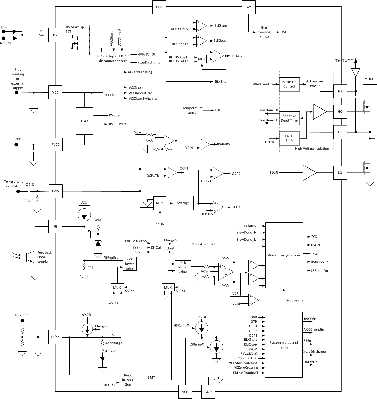
7.3 Feature Description
7.3.1 Hybrid Hysteretic Control
UCC256304 uses a novel control scheme – Hybrid Hysteretic Control (HHC) - to achieve best in class line and load transient performance. The control method makes the compensator very easy to design. The control method also makes light load management easier and more efficient. Improved line transient enables lower bulk capacitor/output capacitor value and saves system cost.
HHC is a control method which combines traditional frequency control and charge control – It is charge control with added frequency compensation ramp. Comparing with traditional frequency control, it changes the power stage transfer function from a 2nd order system to a 1st order system, so that it is very easy to compensate. The control effort is directly related to input current, so the line and load transients are best in class. Comparing with charge control, the hybrid hysteretic control avoids unstable condition by adding in a frequency compensation ramp. The frequency compensation makes the system always stable, and makes the output impedance lower as well. Lower output impedance makes the transient performance better than charge control.
In summary, the problems solved by HHC are:
- Help LLC converters achieve best in class load transient and line transient
- Changes the small-signal transfer function to a 1st order system which is very easy to compensate, and can achieve very high bandwidth
- Inherently stable via frequency compensation
- Makes burst mode control high efficiency optimization much easier
Figure 28 shows the HHC implementation in UCC256304: a capacitor divider (C1 and C2) and two well matched controlled current source.
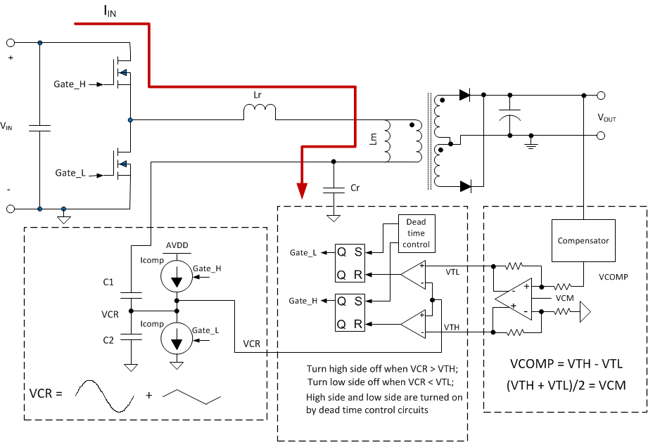 Figure 28. UCC256304 HHC Implementation
The resonant capacitor voltage is divided down by the capacitor divider formed by C1 and C2. The current sources are controlled by the gate drive signals. When high side switch is on, turn on the upper current source to inject a constant current into the capacitor divider; when low side switch is on, turn on the lower current source to pull the same amount of constant current outside of the capacitor divider. The two current sources add a triangular compensation ramp to the VCR node. The current sources are supplied by a reference voltage Vref. This voltage needs to be equal to or larger than twice of the common mode voltage VCM. The divided resonant capacitor voltage and the compensation ramp voltage are then added together to get VCR node voltage. If the frequency compensation ramp dominates, the VCR node voltage will look like a triangular waveform, and the control will be similar to direct frequency control. If the resonant capacitor voltage dominates, the shape of the VCR node voltage will look like the actual resonant capacitor voltage, and the control will be similar to charge control. This is why the control method is called “hybrid” and the compensation ramp is called frequency compensation.
This set up has an inherent negative feedback to keep the high side and low side on time balanced, and also keep the common mode voltage at VCR node at VCM.
There are two input signals needed for the new control scheme: VCR and VCOMP. VCR is the sum of the scaled down version of the resonant capacitor voltage and the frequency compensation ramp. VCOMP is the voltage loop compensator output. The waveform below shows how the high-side and low-side switches are controlled based on VCR and VCOMP. The common mode voltage of VCR is VCM.
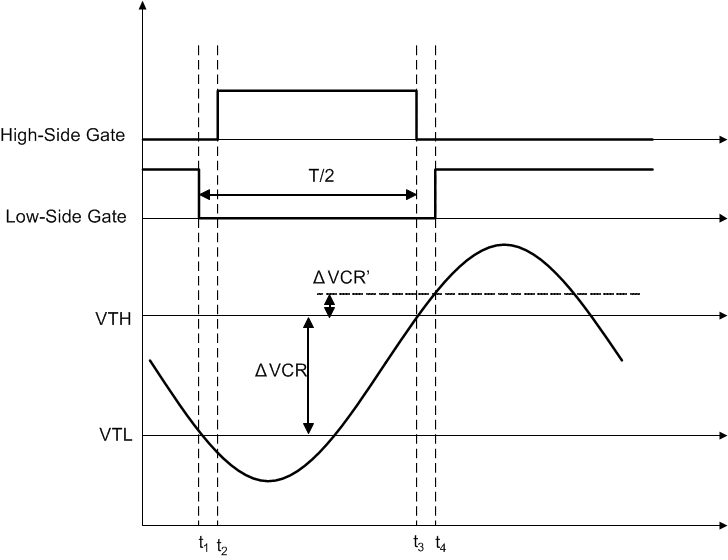 Figure 29. HHC Gate On/Off Control Principle
Based on VCOMP and VCM (3 V), two thresholds: Vthh and Vthl are created.


The VCR voltage is compared with the two thresholds. When VCR > Vthh, turn off high side switch; when VCR < Vthl, turn off low side switch. HO and LO turn on edges are controlled by adaptive dead time circuit.
7.3.2 Regulated 12-V Supply
RVCC pin is the regulated 12-V supply which can supply up to 100-mA current. The regulated rail is used to supply the PFC, and LLC gate driver. RVCC has under voltage lock out (UVLO) function. If during normal operation, RVCC voltage is less than RVCCUVLO threshold. It is treated as a fault and the system will enter FAULT state. Details about the FAULT handling will be discussed in the section.
7.3.3 Feedback Chain
Control of output voltage is provided by a voltage regulator circuit located on the secondary side of the isolation barrier. The demand signal from the secondary regulator circuit is transferred across the isolation barrier using an opto-coupler and is fed into the FB pin on UCC256304. This section discusses about the whole feedback chain.
The feedback chain has the following functions:
- Optocoupler feedback signal input and bias
- System external shut down
- Soft start function selection by a pick lower block
- Burst mode selection by a pick higher block
- Convert single ended feedback demand to two thresholds Vthh and Vthl; and VCR comparison with the thresholds and the common mode voltage VCM
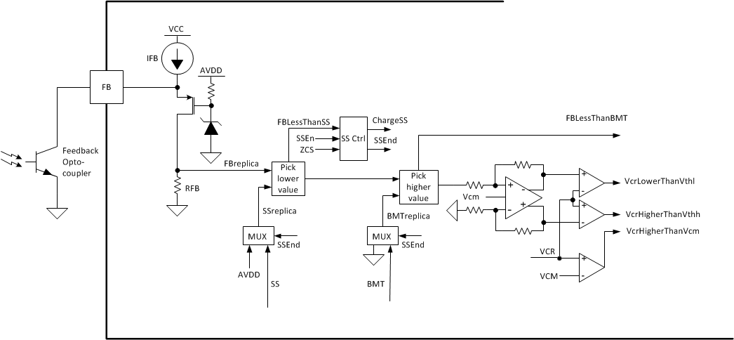 Figure 30. Feedback Chain Block Diagram
The timing diagram below shows the FB chain waveforms. The sequence is normal soft start followed by a ZCS event, and load step into burst mode, and then come out of burst mode.
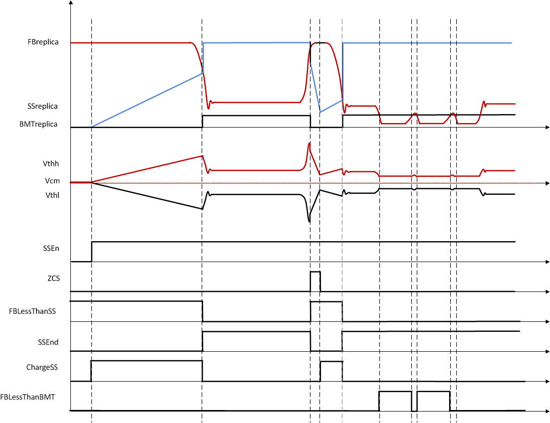 Figure 31. Feedback Chain Timing Diagram
7.3.4 Optocoupler Feedback Signal Input and Bias
The secondary regulator circuit and optocoupler feedback circuit all add directly to the no load power consumed by the system. To achieve very low no load power it is necessary to drive the optocoupler in a low current mode.
As shown in Figure 31, a constant current source IFB is generated out of VCC voltage and connected to FB pin. A resistor RFB is also connected to this current source with a PMOS in series. During normal operation, the PMOS is always on. The PMOS limits the maximum voltage on the FBreplica.

From this equation, when Iopto increases, IRFB will decrease, making FBreplica decrease. In this way, the control effort is inverted. This circuit can also limit the optocoupler maximum current to be IFB. A conventional way to bias the optocoupler is using a pull up resistor on the collector of the optocoupler output. To reduce the power consumption, the pull up resistor needs to be big, which will limit the loop bandwidth. For the bias current method used in UCC256304, the optocoupler current is limited and there is no loop bandwidth issue.
7.3.5 System External Shut Down
This function provides a way to shut down the system by an external signal. When the FBreplica is less than the burst mode threshold, stop LLC switching. When FBLessThanBMT is true for more than 200 ms, go to JFET OFF state and try to re-start. Before LLC starts switching, the system has to make sure that FBLessThanBMT is not true. If FBreplica is constantly held low by an external signal, the system will not start again.
This function can be used for system on/off control or any other fault shut down which isn’t included in UCC256304. To implement this function, an external biased optocoupler is needed. The schematic below is an example of such implementation.
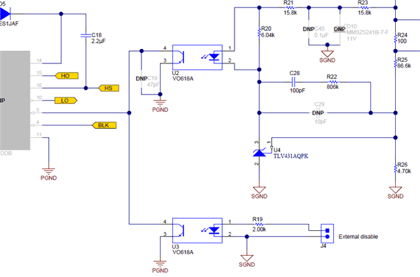 Figure 32. External Disable Example Circuit
7.3.6 Pick Lower Block and Soft Start Multiplexer
This part of the circuit consists of 3 elements:
- A pick lower block
- A MUX which selects AVDD or SS signal as the second input to the pick lower block
- A SS control block which handles the charge and discharge of the SS capacitor in cause of a ZCS fault
The pick lower block has two inputs. The first input is FBreplica. The second input is selected between AVDD and SS pin voltage. The other output of the block is the lower of the two inputs.
The MUX selects between SS and AVDD. The selection is based on SSEnd (soft start end) signal, which is an output of the SS Ctrl block. SSEnd is high when SS is higher than FBreplica, and soft start process has been initiated by the state machine, and there is no ZCS condition. Switching to AVDD after soft start has ended helps make sure that during non-soft start or non-ZCS fault condition, FBreplica signal is always sent through the pick lower block. It also releases the SS pin to do the other function – light load threshold programming.
The SS control block handles the charge and discharge of the SS capacitor in cause of a ZCS fault. It reset the SSEnd signal when ZCS happens, so the effect of pulling down on SS pin to increase the switching frequency can pass through the pick lower block. The relationship of the SS control block inputs and outputs is the following:


7.3.7 Pick Higher Block and Burst Mode Multiplexer
The output of the pick lower block goes into a pick higher block, which selects the higher of the pick lower block output and the burst mode threshold setting.
The burst mode multiplexer selects between BMT and ground. During soft start, the multiplexer selects ground. The startup process is open loop and controlled by the soft start ramp. Burst mode is not enabled during soft start phase.
After soft start, the higher of the two inputs are sent to the differential amplifier. The other output is a comparator output FBLessThanBMT. It is sent to the waveform generator state machine to control burst mode and system external shut down.
7.3.8 VCR Comparators
The output of the pick higher block is sent to a differential amplifier to convert the signal to two thresholds symmetrical to Vcm. The difference between the two thresholds Vthh and Vthl equals the input amplitude. The VCR pin voltage is then compared with Vthh, Vthl, and Vcm. The results are sent to the waveform generator.
7.3.9 Resonant Capacitor Voltage Sensing
The resonant capacitor voltage sense pin senses the resonant capacitor voltage through a capacitor divider. Inside the device, two well matched, controlled current sources are connected to VCR pin to generate the frequency compensation ramp. The on/off control signals in of the two current sources come from the waveform generator block.
During waveform generator IDLE state or before startup, short VCR node to Vcm. This action will help reduce the startup peak current, and help VCR voltage to settle down quickly during burst mode.
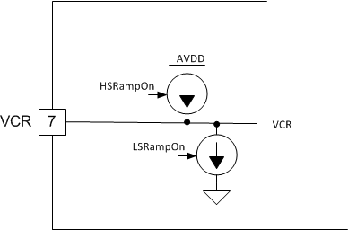 Figure 33. VCR Block Diagram
The ramp current on/off sequence is shown in Figure 34. The ramp current is on all the time. It changes direction at the falling edge of high side on or low side on signal.
 Figure 34. VCR Compensation Ramp Current On/Off
On VCR pin, a capacitor divider is used to mix the resonant capacitor waveform and the compensation ramp waveform. Adjusting the size of the external capacitors can change the contribution of charge control and direct frequency control. Assume the divided down version of the resonant capacitor voltage by the capacitor divider is Vdiv, the compensation ramp current resulted voltage on VCR pin is Vramp. If Vdiv is much larger than Vramp, the control method is similar to charge control, in which the control effort is proportional to the input charge of one switching cycle. If Vramp is much larger than Vdiv, the control method is similar to direct frequency control, in which the control effort is proportional to the switching frequency. The most optimal transient response can be achieved by adjusting the ratio between Vdiv and Vramp.
7.3.10 Resonant Current Sensing
The ISNS pin is connected to the resonant capacitor using a high voltage capacitor. The capacitor CISNS and the resistor RISNS form a differentiator. The resonant capacitor voltage is differentiated to get the resonant current. The differentiated signal is AC and goes both positive and negative. In order to sense the zero crossing, the signal is level shifted using an op amp adder. IPolarity comparator detects the direction of the resonant current. The digital state machine implements a blanking time on IPolarity – IPolarity edges during the first 400ns of dead time are ignored.
OCP2 and OCP3 thresholds are based on average input current. To get the average input current, the differentiator output is multiplexed with the high side switch on signal HSON: when HS is on, the MUX output is the differentiator output; when HS is off, the MUX output is 0. The MUX output is then averaged using a low pass filter. The output of the filter is the sensed average input current. Note that the MUX needs to pass through both positive and negative voltages. OCP2 and OCP3 faults have a 2ms and 50ms timer respectively. Only when the OCP2/OCP3 comparators output high for continuous 2ms or 50ms, the faults will be activated.
OCP1 threshold is set on the peak resonant current. The voltage on the ISNS pin gets compared to OCP1 threshold OCP1Th directly. The peak resonant current is checked once per cycle on the positive half cycle. OCP1 fault is only activated when there are 4 consecutive cycles of OCP1 event detected. During start up, the OCP1 comparator output of the first 15 cycles are ignored.
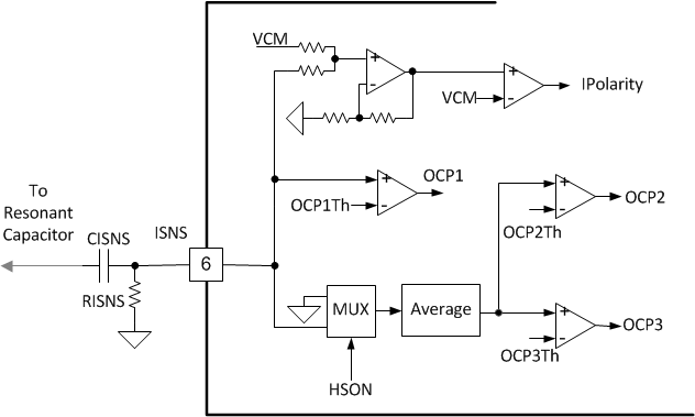 Figure 35. ISNS Block Diagram
7.3.11 Bulk Voltage Sensing
The BLK pin is used to sense the LLC DC input voltage (bulk voltage) level. The comparators on BLK pin set the following thresholds:
- Bulk voltage level when LLC starts switching – BLKStartTh
- Bulk voltage level when LLC stops switching – BLKStopTh
- Bulk voltage level when bulk over voltage fault is generated – BLKOVRiseTh
- Bulk voltage level when bulk over voltage fault is cleared – BLKOVFallTh
BLKOV signal is generated by one comparator with two thresholds selected by a MUX. This is to create necessary hysteresis for the BLKOV fault. The BLKSns signal is buffered and sent to burst mode threshold generation block to implement the adaptive burst mode threshold.
Figure 36 shows the block diagram of the BLK pin.
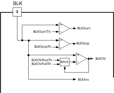 Figure 36. VCR Compensation Ramp Current On/Off
In UCC256304, the BLKOVRiseTh threshold is intentionally made to be much larger than BLKStartTh. This enables the LLC controller to accommodate a very wide DC input voltage range while still maintaining a suitable BLKStopTh. For example, if a startup threshold of 120V is desired, then the BLK resistor divider ratio, kBLK, can be calculated as

For the same BLK resistor divider ratio, the bulk stop voltage is

An over voltage condition occurs when the bulk voltage is greater than or equal to VOVRise

The over voltage condition is cleared when the bulk voltage falls below VOVFall

This wide DC input range offers a number of system level benefits. When UCC256304 is paired with a PFC stage, the LLC converter is able to startup and enter a low power standby mode without the need to enable the PFC. In addition, the wide DC input range enables AC/DC systems to be compatible with an extensive range of common AC Inputs
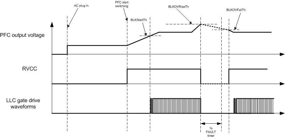 Figure 37. Timing Diagram of BLK Operations
7.3.12 Output Voltage Sensing
The output voltage is sensed through the bias winding (BW) voltage sense pin. The sensed output voltage is compared with a fixed threshold to generate output OVP fault. The block diagram of the bias winding voltage sense block is shown below.
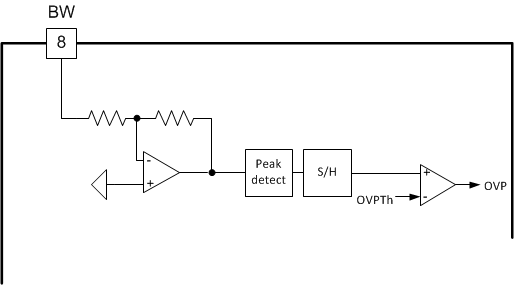 Figure 38. Bias Winding Sensing Block Diagram
The bias winding sense block consists of an inverting op amp to flip the BW signal. The flipped BW signal is then peak detected and sampled at low side turn off edge. The sampled voltage represents the output voltage during this cycle. The S/H output is them compared with OVP comparator. Shown below is the timing diagram of the BW sense block.
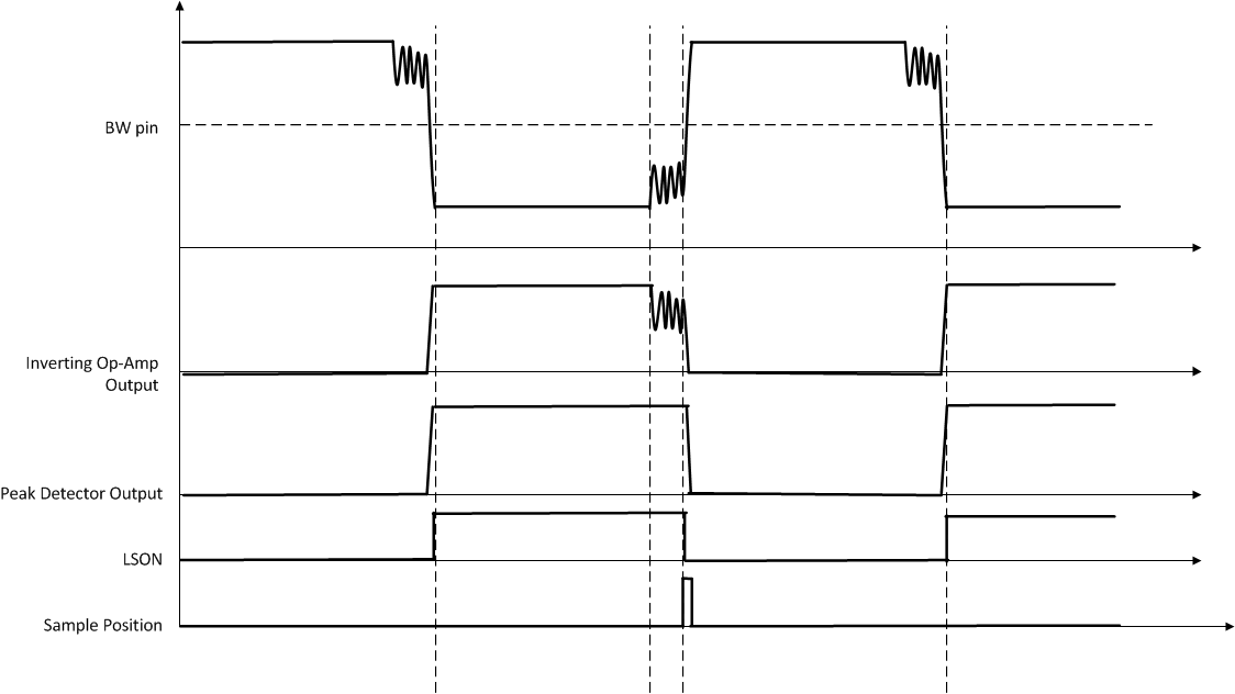 Figure 39. Timing Diagram of BW Sense Block
7.3.13 High Voltage Gate Driver
The low-side gate driver output is LO. The gate driver is supplied by the 12-V RVCC rail.
The high-side driver module consists of three physical device pins. HB and HS form the positive and negative rails, respectively, of the high-side driver, and HO connects to the gate of the upper half-bridge MOSFET.
During periods when the lower half-bridge MOSFET is conducting, HS is shorted to GND via the conducting lower MOSFET. At this time power for the high side driver is obtained from RVCC via high voltage diode DBOOT, and capacitor CBOOT is charged to RVCC minis the forward drop on the diode.
During periods when the upper half-bridge MOSFET is conducting, HS is connected the LLC input voltage rail. At this time the HV diode is reverse biased and the high side driver is powered by charge stored in CBOOT.
The slew on HS pin is detected for adaptive dead time adjustment. The next gate is only turned on when the slew on HS pin is finished.
Both the high-side and low side gate drivers have under voltage lock out (UVLO) protection. The low side gate driver UVLO is implemented on RVCC; the high side gate driver UVLO is implemented on (HB - HS) voltage.
When operating at light load, UCC256304 enters burst mode. During the burst off period, the gate driver enters low power mode to reduce power consumption.
The block diagram of the gate driver is shown in Figure 40.
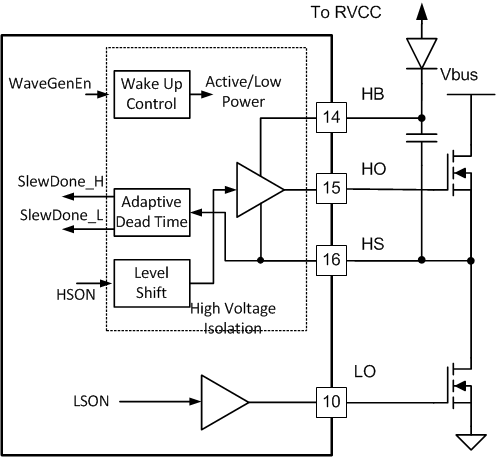 Figure 40. Gate Driver Block Diagram
7.3.14 Protections
7.3.14.1 ZCS Region Prevention
Capacitive region is an LLC operation region in which the voltage gain increases when the switching frequency increases. It is also called ZCS region. Capacitive mode operation should be avoided for two reasons:
- The feedback loop becomes positive feedback in capacitive region
- The MOSFET may be damaged because of body diode reverse recovery
To make sure that capacitive region operation does not happen, we need to first rely on the slew done signal. If there is a slew done signal detected, it suggests that the opposite body diode must not be conducting and to turn on the next FET. If there is no slew detected, IPolarity signal is used. The next gate will be turned on at the next IPolarity flip event. The IPolarity flip indicates that the capacitive operation cycle has already passed. The resonant current reverses the direction and begins to discharge the switch node. When the capacitive operation cycle has passed, the system enters a high frequency oscillation stage, where the oscillation frequency is determined by the parasitic elements in the circuit. In this stage, the body diode is no longer conducting and it is allowed to turn on the next gate.
However, in the high frequency oscillation stage, the resonant current may be so small that the IPolarity detection is missed. In this case, the next gate will be turned on by maximum dead time timer expiration.
In addition to preventing the next gate from turning on when the opposite body diode is conducting, the switching frequency is forced to ramp up until there is a cycle with no capacitive region operation detected
The capacitive region detection is done by checking the resonant current polarity at HSON or LSON falling edge. If the resonant current is positive at LSON falling edge, or negative at HSON falling edge, the ZCS signal in the waveform generator is turned high. The ZCS signal keeps high until there is a half cycle without capacitive region operation happens.
The force ramping up of the switching frequency is done by pull the SS pin down by a resistor to ground. Details will be discussed in SS pin section.
Below is the flow chart of capacitive region prevention algorithm:
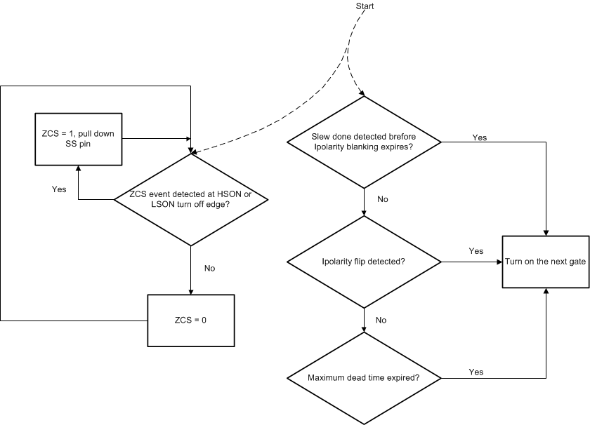 Figure 41. Gate Driver Block Diagram
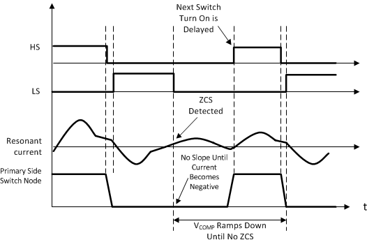 Figure 42. Timing Diagram of a ZCS Event
7.3.14.2 Over Current Protection (OCP)
There are three levels of OCP:
- OCP1: peak current protection (highest threshold)
- Fault action: count OCP1 cycles and shut down power stage if counter exceeds preset value
- OCP2: average input current protection (high threshold)
- Fault action: if above threshold for 2 ms, shut down
- OCP3: average input current protection (low threshold)
- Fault action: if above threshold for 50 ms, shut down
The circuit block diagram has been discussed in the Resonant Current Sensing section.
7.3.14.3 Over Output Voltage Protection (VOUTOVP)
This is the output over voltage protection. VOUTOVP threshold is set on the bias winding voltage sense. The VOUTOVP trip point can be set by configuring the voltage divider on BW pin.
7.3.14.4 Over Input Voltage Protection (VINOVP)
This is the input over voltage protection. The fault actions have been discussed in the BLK section. The trip point can be set by configuring the voltage divider on BLK pin.
7.3.14.5 Under Input Voltage Protection (VINUVP)
This is the input under voltage protection. The fault actions have been discussed in the BLK section. The trip point can be set by configuring the voltage divider on BLK pin.
7.3.14.6 Boot UVLO
This is the high side gate driver UVLO. When (HB – HS) voltage is less than the threshold, the high side gate output will be shut down.
7.3.14.7 RVCC UVLO
This is the regulated 12-V UVLO. When RVCC voltage is less than the threshold, both the high side gate output and the low-side gate output will be turned off.
7.3.14.8 Over Temperature Protection (OTP)
This is the device over temperature protection. When OTP fault is tripped, if the device is switching, the switching will stop. If the device is in HV start up stage and JFET is on, the JFET will be turned off. Details of the OTP fault handling will be discussed in the Device Functional Modes section.
There are two digital state machines in the system:
- System States and Faults State Machine
- Waveform Generator Stage Machine
The system states control state machine controls system operation states and faults. The waveform generator state machine controls the gate driver behavior.
7.4 Device Functional Modes
7.4.1 Burst Mode Control
The efficiency of an LLC converter power stage drops rapidly with falling output power. To maintain reasonable light load efficiency it is necessary to operate the LLC converter in burst mode. In this mode the LLC converter operates at relatively high power for a short burst period and then all switching is stopped for a space period. During the Burst period excess charge is transferred to and stored in the output capacitor. During the Space period this stored charge is used to supply the load current. Providing an effective light-load scheme is a particular problem for an LLC controller that is located on the primary side of the isolation barrier. This is because the feedback demand signal (VCOMP) is mainly a function of input/output voltage ratio and only loosely related to load current. The normal method of placing a couple of thresholds in the VCOMP voltage window to switch OFF and ON the LLC converter does not work effectively. Another issue with the conventional method is that when burst on, the switching pulses are determined by VCOMP, which is usually at initial burst on, and decays as the output voltage rises. The resulting inductor current will be big at first and then decays. This is not optimal because the big current at first may create mechanical vibration. The high switching frequency afterwards may cause two much switching loss.
For an advanced burst mode, the following features are desired:
- The power delivered by each burst should be relatively constant for a certain load.
- The Burst power is set high enough to provide reasonable LLC converter efficiency and low enough to avoid acoustic noise and excessive output voltage ripple.
- When burst on, the average capacitor voltage should settle to VIN/2 as fast as possible for best efficiency.
- The switching frequency or burst power level of each burst pulse should be optimized for efficient operation.
- The burst pattern of each burst should be relatively constant.
- There should be no audible noise.
- Burst mode performance should be consistent across input voltage range.
The HHC method makes the control of the burst mode very straight forward. The block diagram is a functionally accurate description of the burst mode control method in UCC256304.
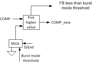 Figure 43. Burst Mode Control Block Diagram
The control effort is selected between the higher of the two signals: 1) the voltage loop compensator output (VCOMP) or 2) the Burst Mode Threshold level (BMT). When VCOMP goes below BMT, continue switching for a fixed number of switching cycles, then stop. Always switch while COMP is higher than BMT. If soft start isn’t done yet, send the COMP (controlled by soft start ramp). BMT is programmable and adaptively changed with input voltage. The last pulse of each burst on period is turned off when the resonant capacitor voltage equals VIN/2. In HHC method, this is approximately equivalent to VCR node voltage equals the common mode voltage VCM. This operation keeps the resonant capacitor voltage to about VIN/2 for each burst off period, thus enabling the burst pattern to settle as soon as possible during burst on period.
7.4.2 High Voltage Start-Up
UCC256304 uses a self bias start up scheme, thus eliminating the need of a separate auxiliary flyback power stage. When AC is first plugged in, PFC and LLC are both off. HV pin JFET will be enabled and will start to deliver current from a source connected to the HV pin to the VCC capacitor. Once the VCC pin voltage exceeds its VCCStartSwitching threshold, the current source will be turned off and RVCC will be enabled to turn on the PFC. When PFC output voltage reaches a certain level, LLC is turned on. When LLC is operating and the output voltage is established, the bias winding will supply current for both the PFC and the LLC controller devicess.
7.4.3 X-Capacitor Discharge
X-capacitors used in EMC filters on the AC side of the diode bridge rectifier must have means to allow them to discharge to a reasonable voltage within certain time, this is to ensure that voltage does not remain present on the pins of the main cord indefinitely.
Typically explicit discharge resistors are provided in parallel with the capacitors to provide this discharge path, but these resistors then lead to fixed standing power loss as long as the power supply is connected to AC, and can be significant in the context of achieving very low standby power.
For every 100 nF of capacitance, a maximum bleed resistor of 10 MΩ must be added in parallel. For a typical 60-W to 100-W power supply with a typical capacitance of 330 nF, this requires 3 MΩ of discharge resistance. At nominal high line 230 V, these resistors dissipate 17.63 mW of standing power loss. Thus it is necessary to find alternative ways to discharge the X-capacitors using switched discharge paths, which avoid the static standing loss.
There are several standards about X-capacitor discharge. IEC60950 and IEC60065 requires that the discharge time constant is less than 1s; IEC62368 requires that after 2 seconds of AC unplug, the remaining voltage on the x-capacitor is less than 60 V (for 300 nF or more capacitance). UCC256304 uses an active discharge scheme to support the fast discharge of up to 5-μF X-capacitor.
To meet the requirements of the standards, AC disconnect event should be detected. UCC256304 detects AC disconnect by monitoring the AC zero crossings through HV pin. When AC is present, there will be two AC zero crossings in one line cycle. When AC is disconnected, there will be no zero crossings for a long time. See Figure 44 shows the rectified AC waveform. In the figure, the AC is disconnected at the peak of the last half AC cycle. In reality, it can be disconnected anywhere in one switching cycle.
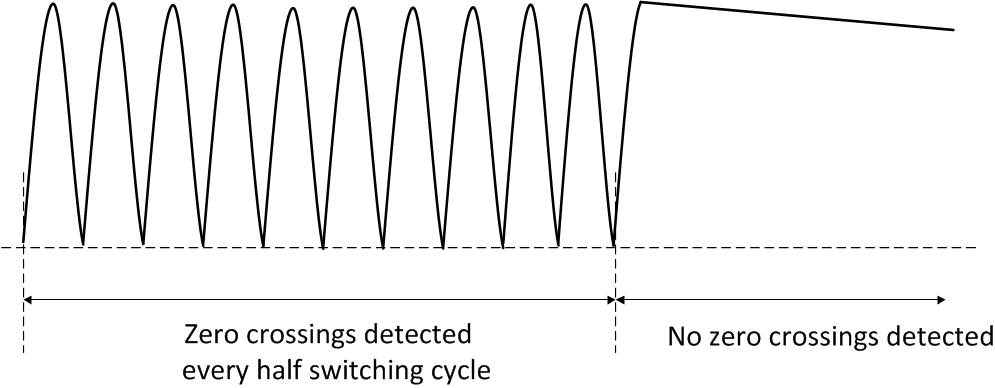 Figure 44. AC Disconnect Waveform
To detect the zero crossings reliably as well as save power consumption, a stair case test current is generated every 700 ms. When there are 4 zero crossings missing in a row at the highest test current setting, AC disconnect is confirmed and the IXCapDischarge current source is enabled. The waveform below shows the stair case current waveform:
 Figure 45. Staircase Test Current for X-Capacitor Discharge
The test current is required for reliable AC zero crossing sensing. In short, this is because the leakage current in the AC bridge rectifier diodes will affect zero crossing detection at very light load. The added test current on HV pin will overcome the leakage current and make sure that AC zero crossing is detected on HV pin. If one zero crossing is detected during any test current stage, it means that AC is not disconnected. The test current will shut off immediately and the system goes to the 700-ms no test current stage.
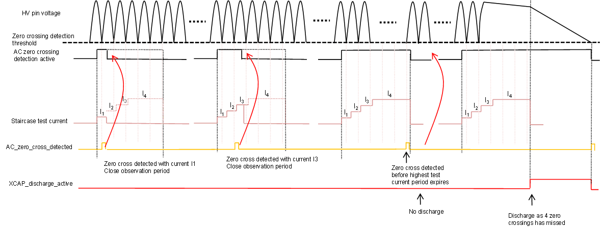 Figure 46. Different Staircase Current Waveforms
Figure 46 shows different staircase current waveforms. The last waveform shows the AC disconnect is detected and x-cap discharge current is enabled. The x-cap discharge current is enabled until 350 ms has passed. AC zero crossing function is available in all operation modes and available all the time. Figure 47 shows the flow chart of AC zero crossing detection and X-capacitor discharge.
The discharge current IXCapDischarge is created by turning on the JFET and enable a current source from JFET source to GND. The reason to discharge to GND rather than discharge to VCC is to prevent VCC from reaching VCCStartSwitching. When AC is unplugged right before an OVP event, the voltage on the VCC is close to reaching VCCStartSwitching.
In LATCH state, the JFET is already on and acts as a pass element for the VCC regulation loop. The switch between the JFET source terminal and VCC pin is closed. If X-cap discharge current source is enabled without disconnect the JFET from the VCC pin, the discharge current has to discharge VCC voltage first, which requires a large amount of current to stay on for a long time. To avoid this issue, in LATCH state, the JFET is disconnected from VCC first. When the discharge phase is finished, turn the switch between JFET and VCC back on. Shown below is the circuit diagram and procedures of x-cap discharge in LATCH state.
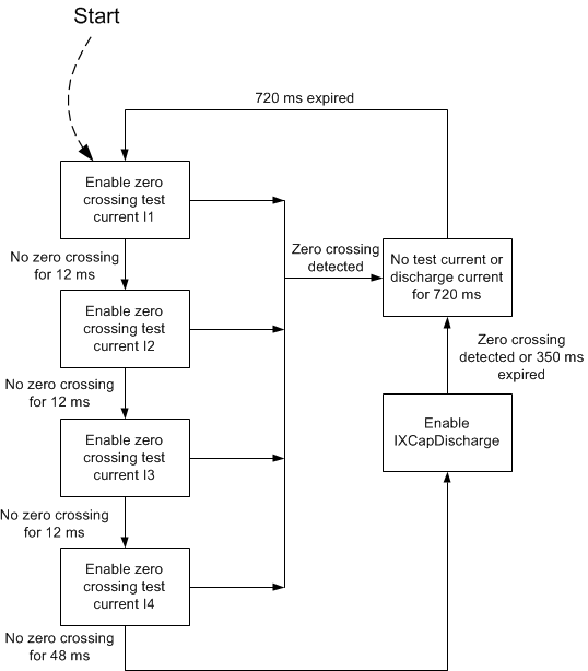 Figure 47. AC ZCD and X-capacitor Discharge Flow Chart
7.4.4 Soft-Start and Burst-Mode Threshold
The soft-start programming and burst mode threshold programming are multiplexed on one pin – LL/SS. In addition, when ZCS region operation happens, this pin is pulled down to ground through a resistor to increase the switching frequency.
An internal constant current source charges the soft start capacitor to generate the soft-start command. Soft start period starts right after charge boot stage is done, and ends when FBreplica becomes lower than SS pin voltage.
After soft start is done, the SS voltage is replaced by AVDD to send to the FB chain. The LL/SS pin is then used to generate the burst mode threshold. In UCC256304 we try to maintain the same burst mode power level over the input voltage range. This is done by adaptively changing the burst mode threshold with sensed BLK voltage.
The programming resistors output provide two degrees of freedom, to set the burst mode threshold, as well as how the threshold changes with BLK voltage. When programmed correctly, the power stage will always enter burst mode at a certain output current level, making the system much easier to optimize.
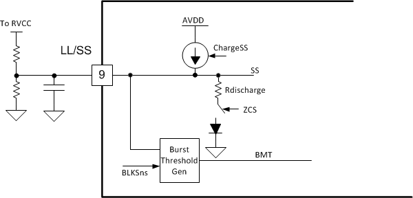 Figure 48. LL/SS Block Diagram
7.4.5 System States and Faults State Machine
Below is an overview of the system states sequence:
The state transition diagram starts from the un-powered condition of UCC256304. As soon as the system is plugged in, HV pin JFET will be enabled and will start to deliver current from a source connected to the HV pin to the VCC capacitor. Once the VCC pin voltage exceeds its VCCStartSwitching threshold, system state will change to JFETOFF. When PFC output voltage reaches a certain level, LLC is turned on. Before LLC starts running, the LO pin is kept high to pull the HS node of the LLC bridge low, thus allowing the capacitor between HB and HS pins to be charged from VCC via the bootstrap diode. UCC256304 will remain in the CHARGE_BOOT state for a certain time to ensure the boot capacitor is fully charged. When LLC output voltage reaches a certain level, both PFC and LLC gets power from LLC transformer bias winding. When the load drops to below a certain level, LLC operates in burst mode
Fault conditions encountered by UCC256304 will cause operation to stop, or paused for a certain period of time followed by an automatic re-start. It is to ensure that while a persistent fault condition is present, it is not possible for UCC256304 or the power converter temperature to continue to rise as a result of the repeated re-start attempts.
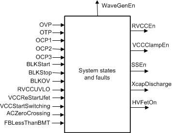 Figure 49. Block Diagram of System States and Faults State Machine
Table 1 summarizes the inputs and outputs of Figure 49
Table 1. System States and Faults State Machine Block Inputs and Outputs
| SIGNAL NAME | I/O | DESCRIPTION |
|---|---|---|
| OVP | I | Output over voltage fault |
| OTP | I | Over temperature fault |
| OCP1 | I | Peak current fault |
| OCP2 | I | Average current fault with 2ms timer |
| OCP3 | I | Average current fault with 50ms timer |
| BLKStart | I | Bulk voltage is above start threshold |
| BLKStop | I | Bulk voltage is below stop threshold |
| BLKOV | I | Bulk over voltage fault |
| RVCCUVLO | I | RVCC UVLO fault |
| VCCReStartJfet | I | VCC is below restart threshold |
| VCCStartSwitching | I | VCC is above start switching threshold (the threshold is different in self bias mode and external bias mode) |
| ACZeroCrossing | I | AC zero crossing is detected |
| FBLessThanBMT | I | FBReplica voltage is less than burst mode threshold |
| WaveGenEn | O | Waveform generator enable |
| RVCCEn | O | RVCC enable |
| VCCClampEn | O | Enable VCC clamp mode (details in VCC pin section) |
| SSEn | O | Soft start enable |
| XcapDischarge | O | Activate x-cap discharge |
| HVFetOn | O | Turn on or off JFET |
The state machine is shown in Figure 50 and the description of the states and state transition conditions are in the tables below.
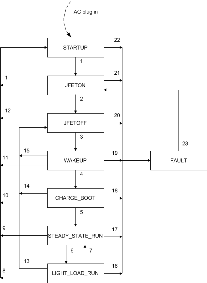 Figure 50. System States and Faults State Machine
Table 2. States in System States and Faults State Machine(1)
| STATE | OUTPUT STATUS | DESCRIPTION |
|---|---|---|
| STARTUP | WaveGenEn = 0 RVCCEn = 0 VCCClampEn = 1 SSEn = 0 HVFetOn = 1 |
This is the first state after power on reset (POR). In this state, the HV JEFT is on, and it’s working in a voltage clamp state where the VCC voltage is regulated to 13V to allow internal circuits to load trim settings and start up. |
| JFETON | WaveGenEn = 0 RVCCEn = 0 VCCClampEn = 0 SSEn = 0 HVFetOn = 1 |
In this state, the JFET is on. The VCC clamp mode is disabled. HV start up current is regulated to IHVHigh. |
| JFETOFF | WaveGenEn = 0 RVCCEn = 1 VCCClampEn = 0 SSEn = 0 HVFetOn = 0 |
When VCC is higher than VCCStartSwitching threshold, the JFET is turned off and system enters JFETOFF state. The regulated RVCC is turned on. PFC soft start begins. |
| WAKEUP | WaveGenEn = 0 RVCCEn = 1 VCCClampEn = 0 SSEn = 0 HVFetOn = 0 |
When BLK voltage reaches BLKStart level, the system enters WAKEUP state and stay in WAKEUP state for 150us for the analog circuits to wake up. |
| CHARGE_BOOT | WaveGenEn = 0 RVCCEn = 1 VCCClampEn = 0 SSEn = 0 HVFetOn = 0 |
In this state, the BOOT capacitor is charged by turning on the low side switch for a certain period of time. |
| STEADY_STATE_RUN | WaveGenEn = 1 RVCCEn = 1 VCCClampEn = 0 SSEn = 1 HVFetOn = 0 |
In this state, the waveform generator is enabled. Soft start module is enabled. LLC starts to soft start. When soft start is done, the system enters normal operation. |
| LIGHT_LOAD_RUN | WaveGenEn = 1 RVCCEn = 1 VCCClampEn = 0 SSEn = 1 HVFetOn = 0 |
If FBReplica is less than burst mode threshold during normal operation, the system enters LIGHT_LOAD_RUN mode. The FBLessThanBMT time is counted. If the time is longer than 200ms, it is treated as a fault, restart the system. |
| FAULT | WaveGenEn = 0 RVCCEn = 0 VCCClampEn = 0 SSEn = 0 HVFetOn = 0 |
After any fault condition, the system enters FAULT state and waits for 1s before re-start. The 1s timer allows system to cool down and prevents frequent repetitive start up in case of a persistent fault. |
Table 3. System States and Faults State Machine State Transition Conditions
| STATE TRANSITION CONDITION | DESCRIPTION |
|---|---|
| 1 | System ready (trim load done) |
| 2 | VCCStartSwitching = 1 VCCReStartJfet = 0 |
| 3 | BLKStart = 1 BLKStop = 0 BLKOV = 0 RVCCUVLO = 0 |
| 4 | BLKStart = 1 BLKStop = 0 BLKOV = 0 RVCCUVLO = 0 FBLessThanBMT = 0 |
| 5 | Charge boot done |
| 6 | FBLessThanBMT = 1 |
| 7 | FBLessThanBMT = 0 |
| 8 | VCCReStartJfet = 1 |
| 9 | VCCReStartJfet = 1 |
| 10 | VCCReStartJfet = 1 |
| 11 | VCCReStartJfet = 1 |
| 12 | VCCReStartJfet = 1 |
| 13 | FBLessThanBMT time out |
| 14 | BLKOV = 1 |
| 15 | BLKOV = 1 |
| 16 | OTP = 1 or BLKOV = 1 or BLKStop = 1 or OVP or OCP1 or OCP2 time out or OCP3 time out or RVCCUVLO = 1 |
| 17 | OTP = 1 or BLKOV = 1 or BLKStop = 1 or OVP or OCP1 or OCP2 time out or OCP3 time out or RVCCUVLO = 1 |
| 18 | OTP = 1 |
| 19 | OTP = 1 |
| 20 | OTP = 1 |
| 21 | OTP = 1 |
| 22 | OTP = 1 |
| 23 | 1s pause time out |
Figure 51 only shows the most commonly used state transition (assuming no faults during start up states so all the states are captured in the timing diagram). Many different ways of state transitions may happen according to the state machine, but are not captured in this section.
In Figure 51, a normal start up procedure is shown. The system enters normal operation and then a fault (OCP, OVP, or OTP) happens.
NOTE
OCP1 and OVP are fast faults and are first processed in the waveform generator state machine.
The system is configured to be restart after 1s pause time.
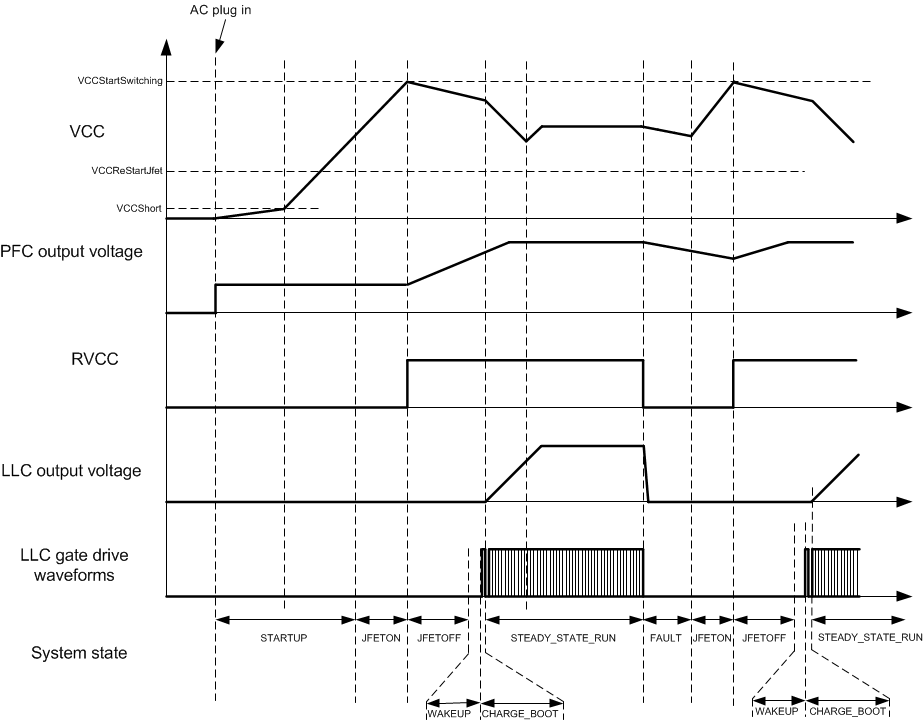 Figure 51. Timing Diagram of System States and Faults
7.4.6 Waveform Generator State Machine
The waveform generator module consists of a state machine that implements hybrid hysteretic control, adaptive dead time, and ZCS protection. Each cycle of LLC operation is broken down into 4 separate periods: HSON, DTHL, LSON, and DTLH. In addition, there is an IDLE state and a WAKEUP state.
The initial state of this state machine is IDLE. In IDLE state, the system is operating in a low power mode. When WaveGenEn command is received, the state machine enters WAKEUP state to turn on various circuit blocks. Once the WAKEUP timer is expired, the system enters LSON (low side on) state. LSON state is followed by DTLH (dead time high to low) state, which is the dead time state. After DTLH state, the high side turns on and system enters HSON. HSON state is followed by DTHL (dead time low to high) state. After DTHL, the system goes back to LSON state again.
There are minimum and maximum timers in each of the states. The state transition conditions and descriptions are discussed in detail below.
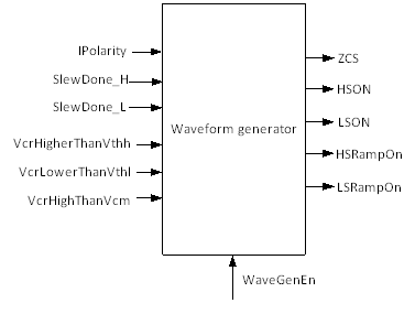 Figure 52. Waveform Generator State Machine Block Diagram
Table 4 summarizes the inputs and outputs of the Waveform Generator State Machine Block Diagram
NOTE
OVP and OCP1 faults are not listed here. But they are processed in the wave gen state machine before handled to system states and faults state machine.
Table 4. Waveform Generator State Machine Inputs and Outputs
| SIGNAL NAME | I/O | DESCRIPTION |
| IPolarity | I | Polarity of the resonant current (Note: this signal has a 1us blanking time during dead time. IPolarity signal listed here is after blanking. See ISNS section for details.) |
| SlewDone_H | I | Primary side switch node completes slewing from low to high |
| SlewDone_L | I | Primary side switch node completes slewing from high to low |
| VcrHigherThanVthh | I | VCR voltage is higher than the high threshold Vthh |
| VcrLowerThanVthl | I | VCR voltage is lower than the low threshold Vthl |
| VcrHighThanVcm | I | VCR voltage is high than the common mode voltage Vcm |
| WaveGenEn | I | Waveform generator enable |
| ZCS | O | Zero current switching is detected |
| HSON | O | High side gate driver on |
| LSON | O | Low side gate driver on |
| HSRampOn | O | High side compensation current ramp on |
| LSRampOn | O | Low side compensation current ramp on |
The state machine is shown in Figure 53 and the description of the states and state transition conditions are in Table 5.
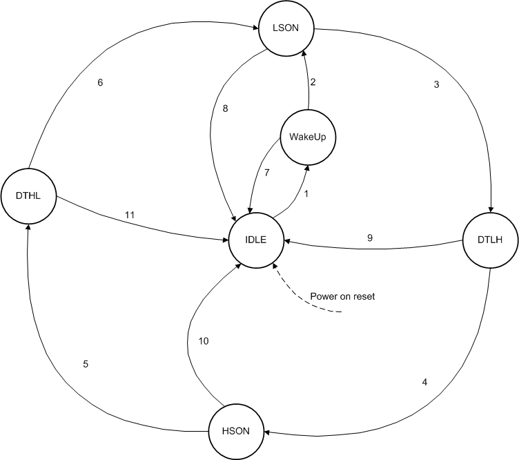 Figure 53. Waveform Generator State Machine
Table 5. States in Waveform Generator State Machine
| STATE | OUTPUT STATUS | DESCRIPTION |
|---|---|---|
| IDLE | HSON = 0 LSON = 0 HSRampOn = 0 LSRampOn = 0 ZCS = 0 |
Both high side and low side are off in this state. Various circuits are operating in low power mode. This is the first state after POR. During burst off period, the system is in IDLE state as well. Upon entering IDLE state, load burst cycle counter, switching cycle counter, OCP1 counter, and OVP counter. Load startup cycle counter if WaveGenEn_Rising = 1 |
| WakeUp | HSON = 0 LSON = 0 HSRampOn = 0 LSRampOn = 0 ZCS = 0 |
In this state, internal circuits wake up from low power mode. |
| LSON | HSON = 0 LSON = 1 HSRampOn = 0 LSRampOn = 1 ZCS = 0 or 1 |
In this state, the low side gate turns on; the low side ramp current source turns on. ZCS may be 0 or 1 depends on the detected result. More details will be described in ZCS section. Enable low side on timer. |
| DTLH | HSON = 0 LSON = 0 HSRampOn = 1 LSRampOn = 0 ZCS = 0 or 1 |
Dead time from low side on to high side on. Low side ramp current source turns off. High side ramp current source turns on. Enable dead time timer. |
| HSON | HSON = 1 LSON = 0 HSRampOn = 1 LSRampOn = 0 ZCS = 0 or 1 |
In this state, the high side gate turns on; the high side ramp current source turns on. ZCS may be 0 or 1 depends on the detected result. More details will be described in ZCS section. Enable high side on timer. |
| DTHL | HSON = 0 LSON = 0 HSRampOn = 0 LSRampOn = 1 ZCS = 0 or 1 |
Dead time from high side on to low side on. High side ramp current source turns off. Low side ramp current source turns on. Enable dead time timer. |
Table 6. Waveform Generator State Machine State Transition Conditions
| STATE TRANSITION CONDITION | DESCRIPTION |
| 1 | WaveGenEn = 1 and FBLessThanBMT = 0 and minimum IDLE time expired |
| 2 | Wake up time expired |
| 3 | (VcrLowerThanVthl = 1 or LSON max timer expired) and LSON min timer expired |
| 4 | StartUpCounterExpired = 0 and DTStartUpTimerExpired = 1 DTMaxTimerExpired = 1 SlewDone_H = 1 SlewDone_H = 1 and MeasuredDTExpired = 1; (Note: this condition and the condition above is selectable using a trim bit, depending on whether dead time measure and match feature is wanted) IPolarityFallingEdgeDetected = 1 |
| 5 | (VcrHigherThanVthh = 1 or HSON max timer expired) and HSON min timer expired |
| 6 | StartUpCounterExpired = 0 and DTStartUpTimerExpired = 1 DTMaxTimerExpired = 1 SlewDone_L = 1 IPolarityFallingEdgeDetected = 1 |
| 7 | WaveGenEn = 0 |
| 8 | WaveGenEn = 0 (VcrLowerThanVthl = 1 or LSON max timer expired) and LSON min timer expired and (OCP1 counter expire or OVP counter expire) |
| 9 | WaveGenEn = 0 |
| 10 | WaveGenEn = 0 BurstModeCountExpire = 1 and VcrHigherThanVcm = 1 and FBLessThanBMT = 1 and HSON min time expired |
| 11 | WaveGenEn = 0 |
Table 7. Waveform Generator State Machine Internal Counters and Timers
| INTERNAL VARIABLE | DESCRIPTION |
| Switching cycle counter | This counter counts the switching cycle |
| OVP counter | Bias Winding Overvoltage counter. The counter decrements every time a Bias Winding Overvoltage occurs |
| Startup counter | Startup Counter. Counter gets set to 15 when wave generator enable toggles from low to high, and then decrements every switching cycle. When the count hits 0, the dead time state is no longer permitted to be exited via the startup dead time expiration. |
| Burst cycle counter | Burst counter. Counter gets set to 15 and then decrements every switching cycle until it hits ‘0’. If FBLessThanBMT = 1 when the counter is ‘0’, the switcher will stop until FBLessThanBMT = 0. |
| OCP1 counter | OCP1 counter. Counter gets set to 4 and then decrements every switching cycle when OCP1 occurs, until it hits ‘0’ |
| Wakeup timer | Wakeup state timer |
| DT max timer | Maximum dead time timer |
| Startup dead time max timer | Dead time max clamp for the first few start up cycles before the startup counter expires |
| Gate on min timer | Minimum gate on time timer |
| Gate on max timer | Maximum gate on time timer |