SLUSDN5D
September 2019 – October 2022
UCC27282-Q1
PRODUCTION DATA
1
Features
2
Applications
3
Description
4
Revision History
5
Pin Configuration and Functions
6
Specifications
6.1
Absolute Maximum Ratings
6.2
ESD Ratings
6.3
Recommended Operating Conditions
6.4
Thermal Information
6.5
Electrical Characteristics
6.6
Switching Characteristics
6.7
Timing Diagrams
6.8
Typical Characteristics
7
Detailed Description
7.1
Overview
7.2
Functional Block Diagram
7.3
Feature Description
7.3.1
Enable
7.3.2
Start-up and UVLO
7.3.3
Input Stages and Interlock
7.3.4
Level Shifter
7.3.5
Output Stage
7.3.6
Negative Voltage Transients
7.4
Device Functional Modes
8
Application and Implementation
8.1
Application Information
8.2
Typical Application
8.2.1
Design Requirements
8.2.2
Detailed Design Procedure
8.2.2.1
Select Bootstrap and VDD Capacitor
8.2.2.2
Estimate Driver Power Losses
8.2.2.3
Selecting External Gate Resistor
8.2.2.4
Delays and Pulse Width
8.2.2.5
External Bootstrap Diode
8.2.2.6
VDD and Input Filter
8.2.2.7
Transient Protection
8.2.3
Application Curves
9
Power Supply Recommendations
10
Layout
10.1
Layout Guidelines
10.2
Layout Example
11
Device and Documentation Support
11.1
Third-Party Products Disclaimer
11.2
Receiving Notification of Documentation Updates
11.3
Support Resources
11.4
Trademarks
11.5
Electrostatic Discharge Caution
11.6
Glossary
Mechanical, Packaging, and Orderable Information
Package Options
Mechanical Data (Package|Pins)
D|8
MSOI002K
DDA|8
MPDS092F
DRC|10
MPDS117L
Thermal pad, mechanical data (Package|Pins)
DDA|8
PPTD178C
DRC|10
QFND013N
Orderable Information
slusdn5d_oa
slusdn5d_pm
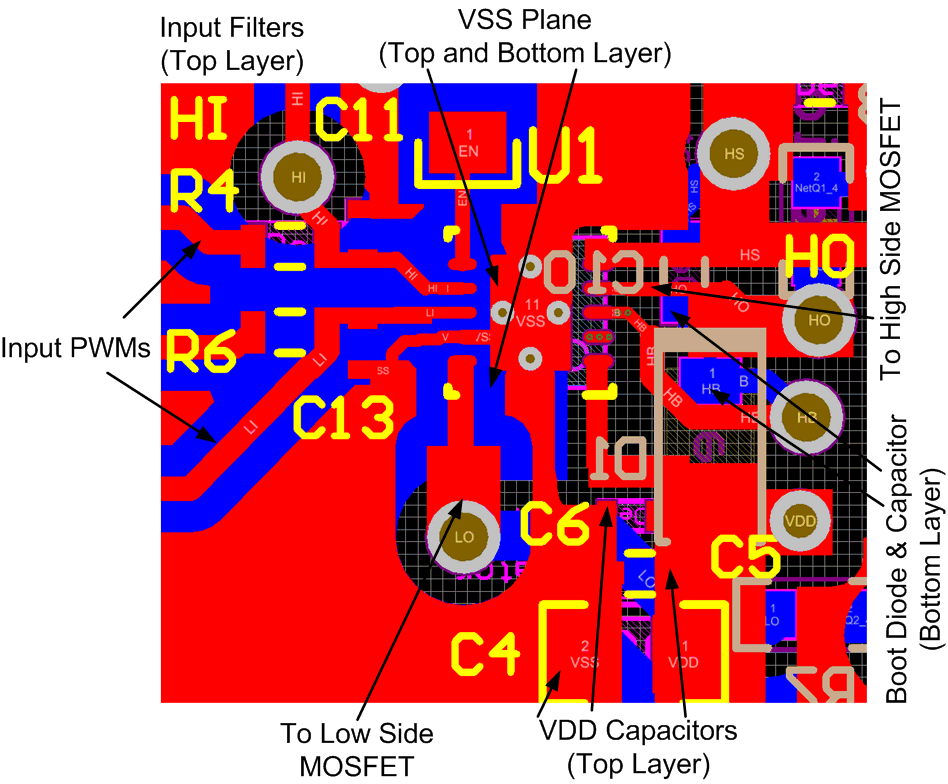
10.2
Layout Example
Figure 10-1
Layout Example