UCC2742x-EP Dual 4-A High-Speed Low-Side MOSFET Driver With Enable
1 Features
- Industry-Standard Pinout
- Enable Functions for Each Driver
- High Current-Drive Capability of ±4 A
- Unique Bipolar and CMOS True-Drive Output Stage Provides High Current at MOSFET Miller Thresholds
- TTL-/CMOS-Compatible Inputs Independent of Supply Voltage
- 20-ns Typical Rise and 15-ns Typical Fall Times With 1.8-nF Load
- Typical Propagation Delay Times of 25 ns With Input Falling and 35 ns With Input Rising
- 4.5-V to 15-V Supply Voltage
- Dual Outputs can be Paralleled for Higher Drive Current
- Available in Thermally-Enhanced MSOP PowerPAD™ Package With 4.7°C/W RθJC
- Supports Defense, Aerospace, and Medical Applications
- Controlled Baseline
- One Assembly/Test Site
- One Fabrication Site
- Extended Product Life Cycle
- Extended Product-Change Notification
- Product Traceability
2 Applications
- Switch-Mode Power Supplies
- DC/DC Converters
- Motor Controllers
- Line Drivers
- Class-D Switching Amplifiers
3 Description
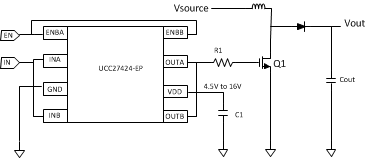
The UCC27423 and UCC27424 high-speed MOSFET drivers can deliver large peak currents into capacitive loads. Two standard logic options are offered – dual inverting and dual noninverting drivers. The UCC27424 thermally-enhanced 8-pin PowerPAD™ MSOP package (DGN) drastically lowers the thermal resistance to improve long-term reliability. The UCC27423 is offered in a standard SOIC-8 (D) package.
Using a design that inherently minimizes shoot-through current, this driver delivers 4 A of current where it is needed most – at the Miller plateau region during the MOSFET switching transition. A unique bipolar and MOSFET hybrid output stage in parallel also allows efficient current sourcing and sinking at low supply voltages.
The UCC27423 and UCC27424 provide enable (ENB) functions to better control the operation of the driver applications. ENBA and ENBB are implemented on pins 1 and 8, which previously were left unused in the industry-standard pinout. ENBA and ENBB are pulled up internally to VDD for active-high logic and can be left open for standard operation.
Device Information(1)
| PART NUMBER | PACKAGE | BODY SIZE (NOM) |
|---|---|---|
| UCC27423-EP | D (8) | 3.91 mm × 4.90 mm |
| UCC27424-EP | DGN (8) | 3.00 mm × 3.00 mm |
- For all available packages, see the orderable addendum at the end of the data sheet.
Simplified Schematic
4 Revision History
Changes from B Revision (April 2012) to C Revision
- Added ESD Ratings table, Feature Description section, Device Functional Modes, Application and Implementation section, Power Supply Recommendations section, Layout section, Device and Documentation Support section, and Mechanical, Packaging, and Orderable Information section Go
Changes from A Revision (November, 2009) to B Revision
- Changed minimum supply voltage from 4-V to 4.5-V in Features sectionGo
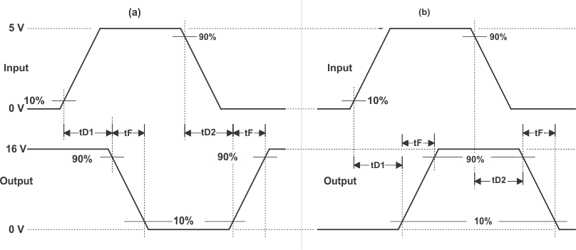
- Changed Figure 11, Rise Time vs Supply VoltageGo
- Changed Figure 12 Fall Time vs Supply Voltage Go
- Changed first paragraph of Operational Waveforms and Circuit Layout sectionGo
- Changed Figure 25, Current SinkingGo
- Changed Figure 26, Current SourcingGo
5 Pin Configuration and Functions
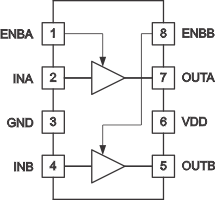
Pin Functions
| PIN | I/O | DESCRIPTION | |
|---|---|---|---|
| NAME | NO. | ||
| ENBA | 1 | I | Enable for driver A with logic-compatible threshold and hysteresis. The driver output can be enabled and disabled with this pin. It is pulled up internally to VDD with a 100-kΩ resistor for active-high operation. When the device is disabled, the output state is low, regardless of the input state. |
| ENBB | 8 | I | Enable for driver B with logic-compatible threshold and hysteresis. The driver output can be enabled and disabled with this pin. It is pulled up internally to VDD with a 100-kΩ resistor for active-high operation. The output state when the device is disabled is low, regardless of the input state. |
| GND | 3 | — | Common ground. This ground should be connected very closely to the source of the power MOSFET that the driver is driving. |
| INA | 2 | I | Input A. Input signal of the A driver, which has logic-compatible threshold and hysteresis. If not used, this input should be tied to either VDD or GND. Do not leave floating. |
| INB | 4 | I | Input B. Input signal of the A driver, which has logic-compatible threshold and hysteresis. If not used, this input should be tied to either VDD or GND. Do not leave floating. |
| OUTA | 7 | O | Driver output A. The output stage is capable of providing 4-A drive current to the gate of a power MOSFET. |
| OUTB | 5 | O | Driver output B. The output stage is capable of providing 4-A drive current to the gate of a power MOSFET. |
| VDD | 6 | I | Supply. Supply voltage and the power input connection for this device. |
6 Specifications
6.1 Absolute Maximum Ratings(1)(2)
over operating free-air temperature range (unless otherwise noted)| MN | MAX | UNIT | ||||
|---|---|---|---|---|---|---|
| VDD | Supply voltage | –0.3 | 16 | V | ||
| Output current | OUTA, OUTB | DC, IOUT_DC | 0.2 | A | ||
| Pulsed (0.5 μs), IOUT_PULSED | 4.5 | |||||
| VIN | Input voltage | INA, INB | –5 | 6 or VDD + 0.3(3) | V | |
| Enable voltage | ENBA, ENBB | –0.3 | 6 or VDD + 0.3(3) | V | ||
| Power dissipation at TA = 25°C | D package | 650 | mW | |||
| DGN package | 3 | W | ||||
| TJ | Junction operating temperature | –55 | 150 | °C | ||
| Lead temperature (soldering, 10 s) | 300 | °C | ||||
| Tstg | Storage temperature | –65 | 150 | °C | ||
6.2 ESD Ratings
| VALUE | UNIT | |||
|---|---|---|---|---|
| V(ESD) | Electrostatic discharge | Human body model (HBM), per ANSI/ESDA/JEDEC JS-001, all pins(1) | ±4000 | V |
| Charged device model (CDM), per JEDEC specification JESD22-C101, all pins(2) | ±1000 | |||
6.3 Recommended Operating Conditions
over operating free-air temperature range (unless otherwise noted)| MIN | MAX | UNIT | ||
|---|---|---|---|---|
| TJ | Operating junction temperature | –55 | 125 | °C |
6.4 Thermal Information
| THERMAL METRIC(1) | UCC27423-EP | UCC27424-EP | UNIT | |
|---|---|---|---|---|
| D | DGN | |||
| 8 PINS | ||||
| RθJA | Junction-to-ambient thermal resistance | 111.4 | °C/W | |
| RθJC(top) | Junction-to-case (top) thermal resistance | 70.8 | ||
| RθJB | Junction-to-board thermal resistance | 56.6 | ||
| ψJT | Junction-to-top characterization parameter | 10.9 | ||
| ψJB | Junction-to-board characterization parameter | 56.1 | ||
6.5 Power Dissipation Ratings
| PACKAGE | SUFFIX | RθJC
(°C/W) |
RθJA
(°C/W) |
POWER RATING (mW) TA = 70°C |
DERATING FACTOR ABOVE 70°C (mW/°C) |
|---|---|---|---|---|---|
| MSOP-8 PowerPAD(3) | DGN | 4.7 | 50 to 59 | 1370(1) | 17.1(1) |
| SOIC 8 | D | 42 | 84 to 160 | 344 to 655(2)(4) | 6.25 to 11.9(2)(4) |
6.6 Electrical Characteristics
VDD = 4.5 V to 15 V, TA = –55°C to 125°C, TA = TJ (unless otherwise noted)| PARAMETER | TEST CONDITIONS | UCC27423 | UCC27424 | UNIT | |||||||
|---|---|---|---|---|---|---|---|---|---|---|---|
| MIN | TYP | MAX | MIN | TYP | MAX | ||||||
| INPUT (INA, INB) | |||||||||||
| VIN_H | Logic 1 input threshold | 2 | 2 | V | |||||||
| VIN_L | Logic 0 input threshold | 1 | 1 | V | |||||||
| Input current | 0 V ≤ VIN ≤ VDD | –10 | 0 | 10 | –10 | 0 | 10 | μA | |||
| OUTPUT (OUTA, OUTB) | |||||||||||
| Output current | VDD = 14 V(1)(2) | 4 | 4 | A | |||||||
| VOH | High-level output voltage | VOH = VDD – VOUT, IOUT = –10 mA | 330 | 450 | 330 | 450 | mV | ||||
| VOL | Low-level output level | IOUT = 10 mA | 22 | 40 | 22 | 40 | mV | ||||
| Output resistance high | IOUT = –10 mA, VDD = 14 V(3) | TA = 25°C | 25 | 30 | 35 | 25 | 30 | 35 | Ω | ||
| TA = full range | 14 | 45 | 18 | 45 | |||||||
| Output resistance low | IOUT = –10 mA, VDD = 14 V(3) | TA = 25°C | 1.9 | 2.2 | 2.5 | 1.9 | 2.2 | 2.5 | Ω | ||
| TA = full range | 0.95 | 4 | 1.2 | 4 | |||||||
| Latch-up protection(1) | 500 | 500 | mA | ||||||||
| SWITCHING TIME | |||||||||||
| tR | Rise time (OUTA, OUTB) | CLOAD = 1.8 nF(1) | 20 | 40 | 20 | 40 | ns | ||||
| tF | Fall time (OUTA, OUTB) | CLOAD = 1.8 nF(1) | 15 | 40 | 15 | 40 | ns | ||||
| tD1 | Delay, IN rising (IN to OUT) | CLOAD = 1.8 nF(1) | 35 | 55 | 35 | 50 | ns | ||||
| tD2 | Delay, IN falling (IN to OUT) | CLOAD = 1.8 nF(1) | 25 | 60 | 25 | 45 | ns | ||||
| ENABLE (ENBA, ENBB) | |||||||||||
| VIN_H | High-level input voltage | Low-to-high transition | 1.7 | 2.4 | 3.1 | 1.7 | 2.4 | 2.9 | V | ||
| VIN_L | Low-level input voltage | High-to-low transition | 1.1 | 1.8 | 2.3 | 1.1 | 1.8 | 2.2 | V | ||
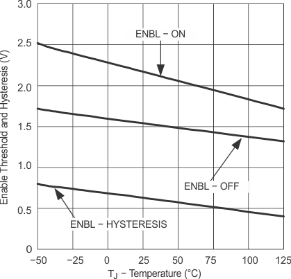
| Hysteresis | 0.13 | 0.55 | 1.1 | .10 | 0.55 | 0.9 | V | ||||
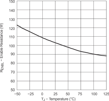
| RENBL | Enable impedance | VDD = 14 V, | ENBL = GND | 75 | 100 | 160 | 75 | 100 | 140 | kΩ | |
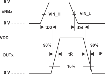
| tD3 | Propagation delay time(4) | CLOAD = 1.8 nF(1) | 30 | 60 | 30 | 60 | ns | ||||
| tD4 | Propagation delay time(4) | CLOAD = 1.8 nF(1) | 100 | 150 | 100 | 150 | ns | ||||
| OVERALL | |||||||||||
| IDD | Static operating current, VDD = 15 V, ENBA = ENBB = 15 V |
INA = 0 V | INB = 0 V | 900 | 1350 | 300 | 450 | μA | |||
| INB = High | 750 | 1100 | 750 | 1100 | |||||||
| INA = HIGH | INB = 0 V | 750 | 1100 | 750 | 1100 | ||||||
| INB = High | 600 | 900 | 1200 | 1800 | |||||||
| Disabled, VDD = 15 V, ENBA = ENBB = 0 V |
INA = 0 V | INB = 0 V | 300 | 450 | 300 | 450 | |||||
| INA = High | 450 | 700 | 450 | 700 | |||||||
| INA = HIGH | INB = 0 V | 450 | 700 | 450 | 700 | ||||||
| INB = High | 600 | 900 | 600 | 900 | |||||||
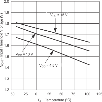
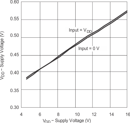
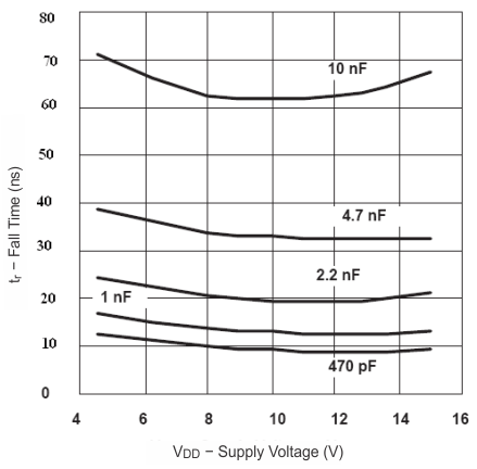
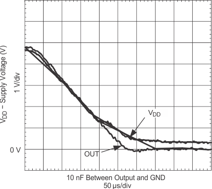
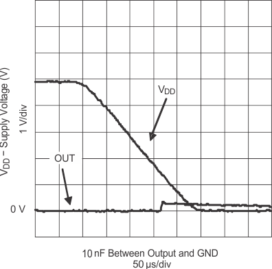
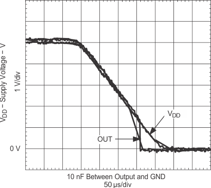
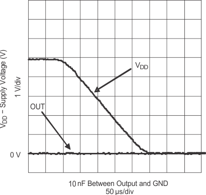
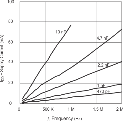
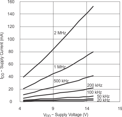
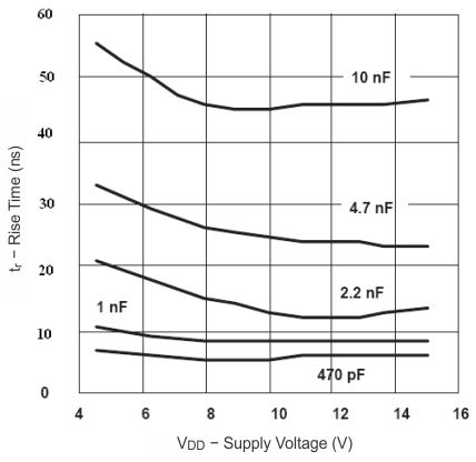
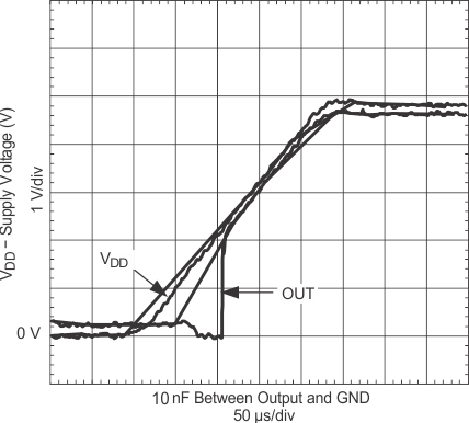
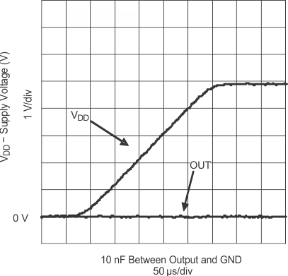
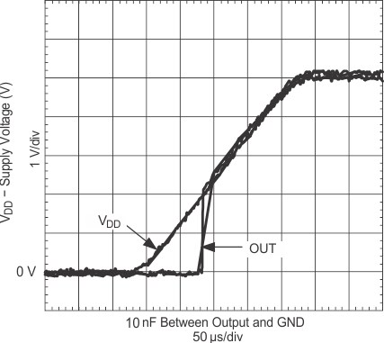
6.7 Typical Characteristics
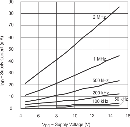
(CLOAD = 2.2 nF)
| IN = GND | ENBL = VDD | |
| IN = VDD | ENBL = VDD | |
| IN = VDD | ENBL = VDD | |
| IN = GND | ENBL = VDD | |
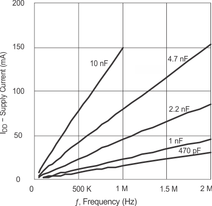
(CLOAD = 4.7 nF)
| IN = GND | ENBL = VDD | |
| IN = VDD | ENBL = VDD | |
| IN = VDD | ENBL = VDD | |
| IN = GND | ENBL = VDD | |