SLUSAY4D March   2012  – December 2014 UCC27516 , UCC27517

PRODUCTION DATA.  

  1. Features
  2. Applications
  3. Description
  4. Revision History
  5. Description (continued)
  6. Device Comparison Table
  7. Pin Configuration and Functions
  8. Specifications
    1. 8.1 Absolute Maximum Ratings
    2. 8.2 ESD Ratings
    3. 8.3 Recommended Operating Conditions
    4. 8.4 Thermal Information
    5. 8.5 Electrical Characteristics
    6. 8.6 Switching Characteristics
    7. 8.7 Typical Characteristics
  9. Detailed Description
    1. 9.1 Overview
    2. 9.2 Functional Block Diagrams
    3. 9.3 Feature Description
      1. 9.3.1 VDD and Undervoltage Lockout
      2. 9.3.2 Operating Supply Current
      3. 9.3.3 Input Stage
      4. 9.3.4 Enable Function
      5. 9.3.5 Output Stage
      6. 9.3.6 Low Propagation Delays
    4. 9.4 Device Functional Modes
  10. 10Application and Implementation
    1. 10.1 Application Information
    2. 10.2 Typical Application
      1. 10.2.1 Design Requirements
      2. 10.2.2 Detailed Design Procedure
        1. 10.2.2.1 Input-to-Output Logic
        2. 10.2.2.2 Input Threshold Type
        3. 10.2.2.3 VDD Bias Supply Voltage
        4. 10.2.2.4 Peak Source and Sink Currents
        5. 10.2.2.5 Enable and Disable Function
        6. 10.2.2.6 Propagation Delay
      3. 10.2.3 Application Curves
  11. 11Power Supply Recommendations
  12. 12Layout
    1. 12.1 Layout Guidelines
    2. 12.2 Layout Example
    3. 12.3 Thermal Considerations
    4. 12.4 Power Dissipation
  13. 13Device and Documentation Support
    1. 13.1 Related Links
    2. 13.2 Trademarks
    3. 13.3 Electrostatic Discharge Caution
    4. 13.4 Glossary
  14. 14Mechanical, Packaging, and Orderable Information

Package Options

Mechanical Data (Package|Pins)
Thermal pad, mechanical data (Package|Pins)
Orderable Information

7 Pin Configuration and Functions

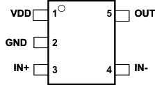
5-Pin
UCC27517 DBV Package
Top View
pin_lusay4.gif
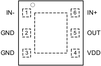
6-Pin
UCC27516 DRS
Top View
pin2_lusay4.gif

Pin Functions – UCC27516

PIN I/O DESCRIPTION
NO. NAME
1 IN– I Inverting Input: When the driver is used in noninverting configuration, connect IN- to GND in order to enable output, OUT held LOW if IN- is unbiased or floating.
2, 3 GND Ground: All signals referenced to this pin. TI recommends to connect pin 2 and pin 3 on PCB as close to the device as possible.
4 VDD I Bias supply input.
5 OUT I Sourcing/Sinking Current Output of Driver
6 IN+ O Noninverting Input: When the driver is used in inverting configuration, connect IN+ to VDD in order to enable output, OUT held LOW if IN+ is unbiased or floating.

Pin Functions – UCC27517

PIN I/O DESCRIPTION
NO. NAME
1 VDD I Bias supply input.
2 GND Ground. All signals reference to this pin. For the UCC27516, TI recommends to connect pin 2 and pin 3 on PCB as close to the device as possible.
3 IN+ I Noninverting input. When the driver is used in inverting configuration, connect IN+ to VDD in order to enable output, OUT held LOW if IN+ is unbiased or floating
4 IN– I Inverting input. When the driver is used in noninverting configuration, connect IN- to GND in order to enable output, OUT held LOW if IN- is unbiased or floating
5 OUT O Sourcing/Sinking current output of driver.