SLUSBA7G December   2012  – June 2019 UCC27531 , UCC27533 , UCC27536 , UCC27537 , UCC27538

PRODUCTION DATA.  

  1. Features
  2. Applications
  3. Description
    1.     Device Images
      1.      Driving IGBT Without Negative Bias
  4. Revision History
    1.     Description (continued)
  5. Device Comparison Table
  6. Pin Configuration and Functions
    1.     Pin Functions
  7. Specifications
    1. 7.1 Absolute Maximum Ratings
    2. 7.2 ESD Ratings
    3. 7.3 Recommended Operating Conditions
    4. 7.4 Thermal Information
    5. 7.5 Electrical Characteristics
    6. 7.6 Switching Characteristics
    7. 7.7 Timing Diagrams
    8. 7.8 Typical Characteristics
  8. Detailed Description
    1. 8.1 Overview
    2. 8.2 Functional Block Diagrams
    3. 8.3 Feature Description
      1. 8.3.1 VDD Undervoltage Lockout
      2. 8.3.2 Input Stage
      3. 8.3.3 Enable Function
      4. 8.3.4 Output Stage
    4. 8.4 Device Functional Modes
  9. Applications and Implementation
    1. 9.1 Application Information
    2. 9.2 Typical Application
      1. 9.2.1 Driving IGBT Without Negative Bias
        1. 9.2.1.1 Design Requirements
        2. 9.2.1.2 Detailed Design Procedure
          1. 9.2.1.2.1 Input-to-Output Configuration
          2. 9.2.1.2.2 Input Threshold Type
          3. 9.2.1.2.3 VDD Bias Supply Voltage
          4. 9.2.1.2.4 Peak Source and Sink Currents
          5. 9.2.1.2.5 Enable and Disable Function
          6. 9.2.1.2.6 Propagation Delay
          7. 9.2.1.2.7 Power Dissipation
        3. 9.2.1.3 Application Curve
      2. 9.2.2 Driving IGBT With 13-V Negative Turn-Off BIAS
        1. 9.2.2.1 Design Requirements
        2. 9.2.2.2 Detailed Design Procedure
        3. 9.2.2.3 Application Curve
      3. 9.2.3 Single-Output Driver
        1. 9.2.3.1 Design Requirements
        2. 9.2.3.2 Detailed Design Procedure
        3. 9.2.3.3 Application Curve
      4. 9.2.4 Using UCC2753x Drivers in an Inverter
        1. 9.2.4.1 Design Requirements
        2. 9.2.4.2 Detailed Design Procedure
        3. 9.2.4.3 Application Curve
  10. 10Power Supply Recommendations
  11. 11Layout
    1. 11.1 Layout Guidelines
    2. 11.2 Layout Example
    3. 11.3 Thermal Consideration
  12. 12Device and Documentation Support
    1. 12.1 Related Links
    2. 12.2 Trademarks
    3. 12.3 Electrostatic Discharge Caution
    4. 12.4 Glossary
  13. 13Mechanical, Packaging, and Orderable Information

Package Options

Mechanical Data (Package|Pins)
Thermal pad, mechanical data (Package|Pins)
Orderable Information

Typical Characteristics

If not specified, INPUT refers to non-inverting input
UCC27531 UCC27533 UCC27536 UCC27537 UCC27538 C001_SLUSBA7.gif
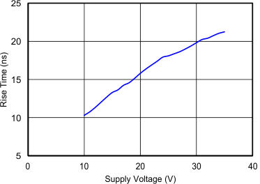
CLOAD = 1.8 nF
Figure 4. Rise Time vs. Supply Voltage
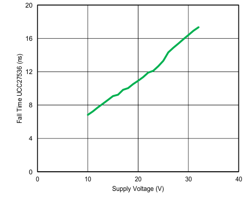
UCC27531 UCC27533 UCC27536 UCC27537 UCC27538 C001_revC_LUSBA7.gif
CLOAD = 1.8 nF
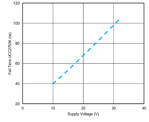
Figure 6. UCC27536 Fall Time vs. Supply Voltage
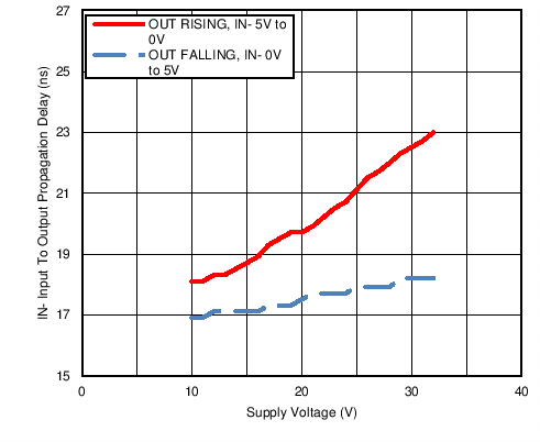
UCC27531 UCC27533 UCC27536 UCC27537 UCC27538 C007a_SLVSBA7C.png
Figure 8. IN- Propagation Delay vs. Supply
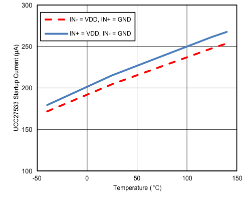
UCC27531 UCC27533 UCC27536 UCC27537 UCC27538 C005_SLUSBA7.gif
VDD = 7 V
Figure 10. UCC27533 Start-Up Current vs. Temperature
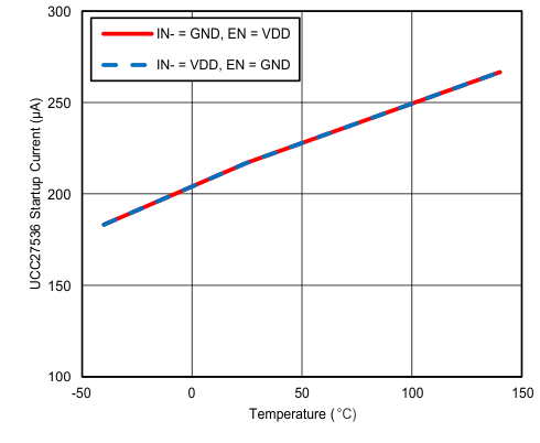
UCC27531 UCC27533 UCC27536 UCC27537 UCC27538 C004_revC_LUSBA7.gif
VDD = 7 V
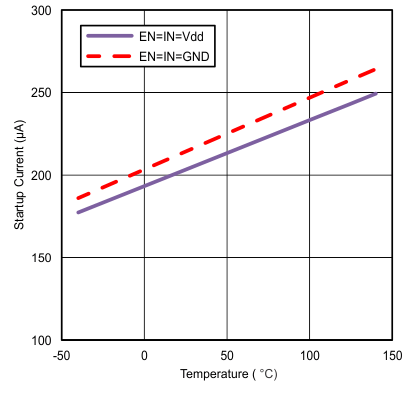
Figure 12. UCC27536 Start-Up Current vs. Temperature
UCC27531 UCC27533 UCC27536 UCC27537 UCC27538 C005_revC_LUSBA7.gif
VDD = 7 V
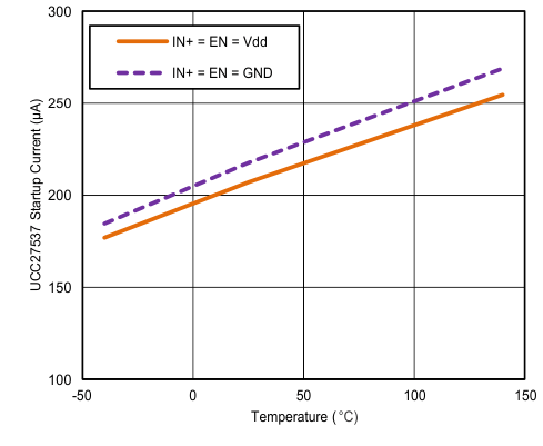
Figure 14. UCC27537 Start-Up Current vs. Temperature
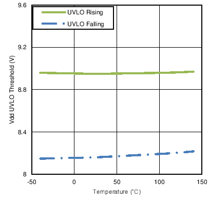
UCC27531 UCC27533 UCC27536 UCC27537 UCC27538 C007_SLUSBA7.pngFigure 16. UVLO Threshold Voltage vs. Temperature
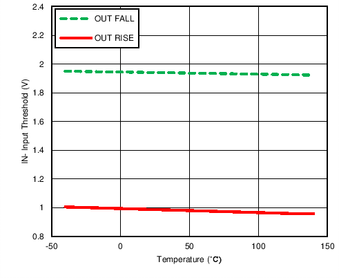
UCC27531 UCC27533 UCC27536 UCC27537 UCC27538 C012a_SLVSBA7C.pngFigure 18. In- Input Threshold vs. Temperature
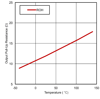
UCC27531 UCC27533 UCC27536 UCC27537 UCC27538 C010_SLUSBA7.gif
VDD = 18 V
Figure 20. Output Pullup Resistance vs. Temperature
UCC27531 UCC27533 UCC27536 UCC27537 UCC27538 C012_SLUSBA7.gif
VDD = 18 V
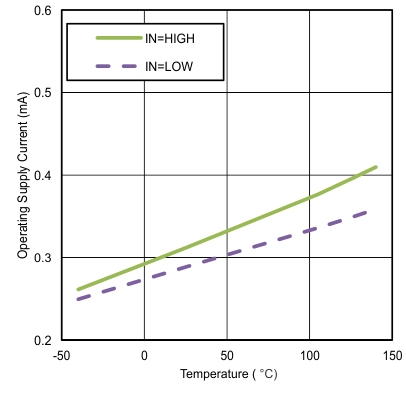
Figure 22. Operating Supply Current vs. Temperature (Output In DC On/Off Condition)
UCC27531 UCC27533 UCC27536 UCC27537 UCC27538 C017a_SLVSBA7C.gif
VDD = 18 V
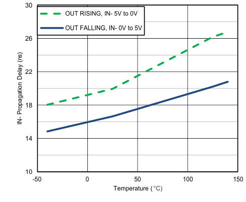
Figure 24. IN– Input-To-Output Propagation Delay vs. Temperature
UCC27531 UCC27533 UCC27536 UCC27537 UCC27538 C015_SLUSBA7.gif
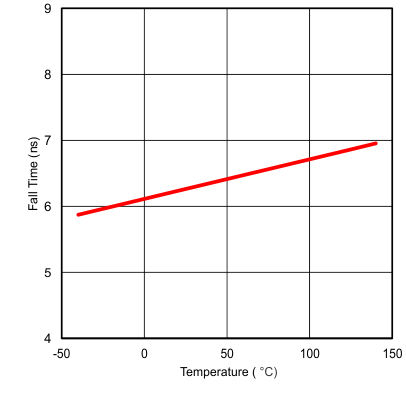
CLOAD = 1.8 nF VDD = 18 V
Figure 26. Fall Time vs. Temperature
UCC27531 UCC27533 UCC27536 UCC27537 UCC27538 C016_SLUSBA7.gif
CLOAD = 1.8 nF VDD = 18 V
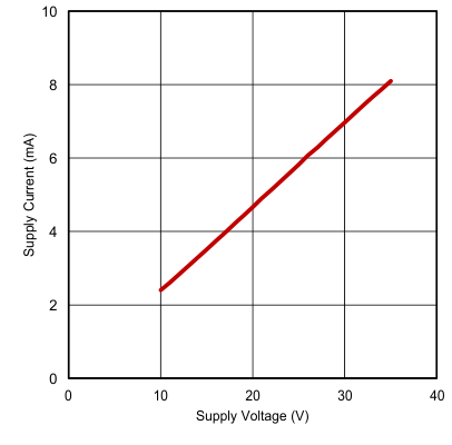
Figure 28. Operating Supply Current vs. Supply Voltage (Output Switching)
UCC27531 UCC27533 UCC27536 UCC27537 UCC27538 C018_SLUSBA7.gif
CLOAD = 1.8 nF
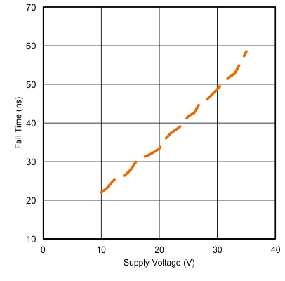
Figure 30. Fall Time vs. Supply Voltage
UCC27531 UCC27533 UCC27536 UCC27537 UCC27538 C002_SLUSBA7.gif
CLOAD = 1.8 nF
Figure 5. Fall Time vs. Supply Voltage
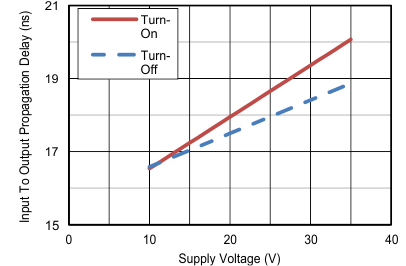
UCC27531 UCC27533 UCC27536 UCC27537 UCC27538 C003_SLUSBA7.gif
Figure 7. Propagation Delay vs. Supply Voltage
UCC27531 UCC27533 UCC27536 UCC27537 UCC27538 newfig8_SLUSBA7.gif
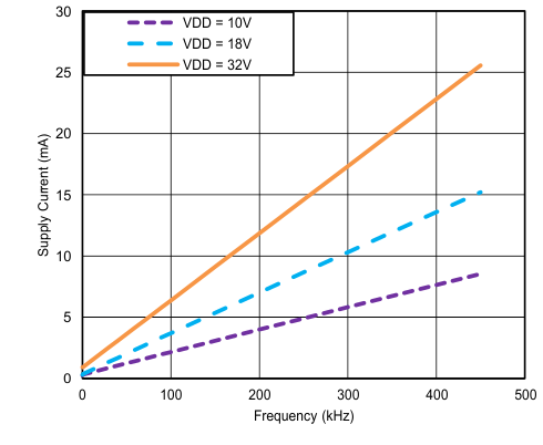
CLOAD = 1.8 nF
Figure 9. Operating Supply Current vs. Frequency
UCC27531 UCC27533 UCC27536 UCC27537 UCC27538 new21curve_SLUSBA7.gif
VDD = 7 V
Figure 11. UCC27531 Start-Up Current vs. Temperature
UCC27531 UCC27533 UCC27536 UCC27537 UCC27538 newcurve23_SLUSBA7.gif
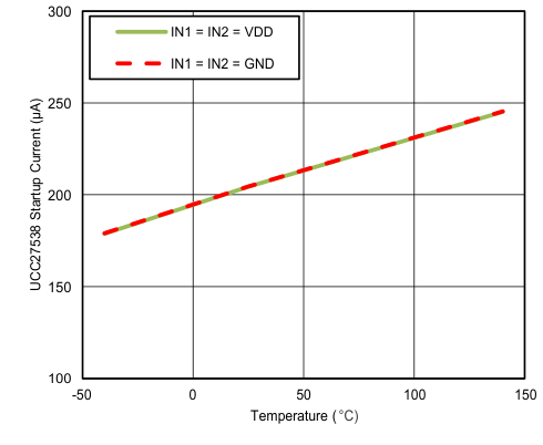
VDD = 7 V
Figure 13. UCC27538 Start-Up Current vs. Temperature
UCC27531 UCC27533 UCC27536 UCC27537 UCC27538 C006_SLUSBA7.gif
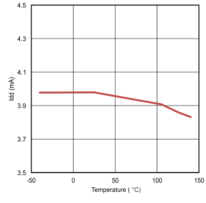
CLOAD = 1.8 nF VDD = 7 V fSW = 100 kHz
Figure 15. Operating Supply Current vs. Temperature (Output Switching)
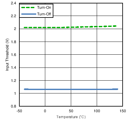
UCC27531 UCC27533 UCC27536 UCC27537 UCC27538 C008_SLUSBA7.pngFigure 17. Input Threshold vs. Temperature
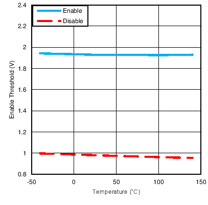
UCC27531 UCC27533 UCC27536 UCC27537 UCC27538 C009_SLUSBA7.pngFigure 19. Enable Threshold vs. Temperature
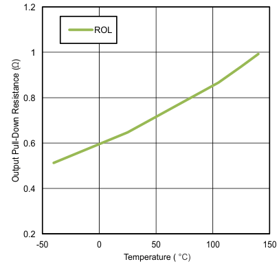
UCC27531 UCC27533 UCC27536 UCC27537 UCC27538 C011_SLUSBA7.gif
VDD = 18 V
Figure 21. Output Pulldown Resistance vs. Temperature
UCC27531 UCC27533 UCC27536 UCC27537 UCC27538 C013_SLUSBA7.gif
VDD = 18 V
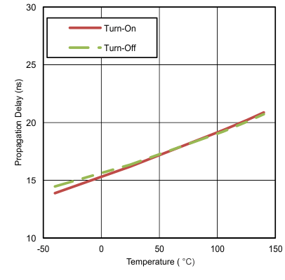
Figure 23. Input-To-Output Propagation Delay vs. Temperature
UCC27531 UCC27533 UCC27536 UCC27537 UCC27538 C014_SLUSBA7.gif
CLOAD = 1.8 nF VDD = 18 V
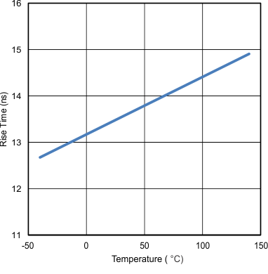
Figure 25. Rise Time vs. Temperature
UCC27531 UCC27533 UCC27536 UCC27537 UCC27538 C003_revC_LUSBA7.gif
CLOAD = 1.8 nF VDD = 18 V
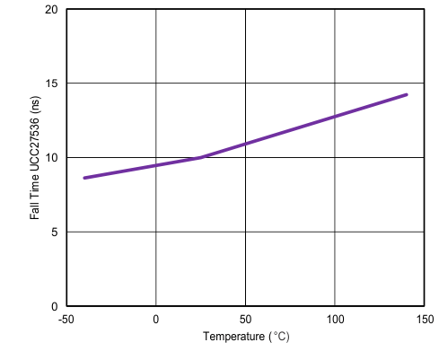
Figure 27. UCC27536 Fall Time vs. Temperature
UCC27531 UCC27533 UCC27536 UCC27537 UCC27538 C017_SLUSBA7.png
CLOAD = 1.8 nF
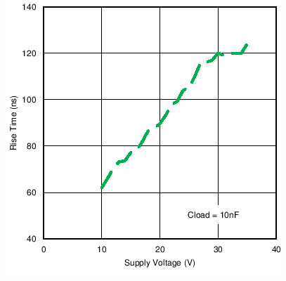
Figure 29. Rise Time vs. Supply Voltage
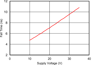
UCC27531 UCC27533 UCC27536 UCC27537 UCC27538 C002_revC_LUSBA7.gif
CLOAD = 1.8 nF
Figure 31. UCC27536 Fall Time vs. Supply Voltage