SLUSCE9B June 2017 – March 2020 UCC27712
PRODUCTION DATA.
- 1 Features
- 2 Applications
- 3 Description
- 4 Revision History
- 5 Pin Configuration and Functions
- 6 Specifications
- 7 Detailed Description
-
8 Application and Implementation
- 8.1 Application Information
- 8.2
Typical Application
- 8.2.1 Design Requirements
- 8.2.2
Detailed Design Procedure
- 8.2.2.1 Selecting HI and LI Low Pass Filter Components (RHI, RLI, CHI, CLI)
- 8.2.2.2 Selecting Bootstrap Capacitor (CBOOT)
- 8.2.2.3 Selecting VDD Bypass/Holdup Capacitor (CVDD) and Rbias
- 8.2.2.4 Selecting Bootstrap Resistor (RBOOT)
- 8.2.2.5 Selecting Gate Resistor RON/ROFF
- 8.2.2.6 Selecting Bootstrap Diode
- 8.2.2.7 Estimate the UCC27712 Power Losses (PUCC27712)
- 8.2.2.8 Estimating Junction Temperature
- 8.2.2.9 Operation With IGBT's
- 8.2.3 Application Curves
- 9 Power Supply Recommendations
- 10Layout
- 11Device and Documentation Support
- 12Mechanical, Packaging, and Orderable Information
Package Options
Mechanical Data (Package|Pins)
- D|8
Thermal pad, mechanical data (Package|Pins)
Orderable Information
8.2.2.9 Operation With IGBT's
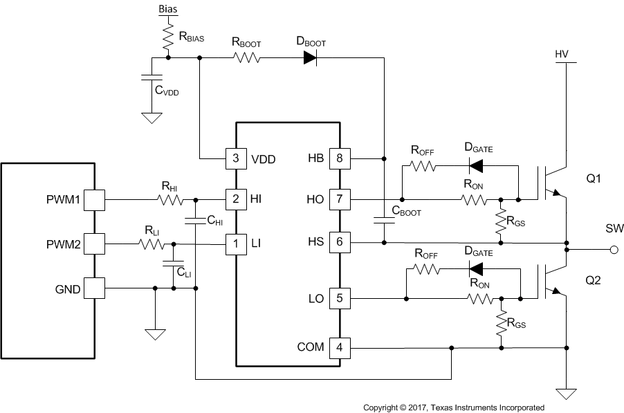
The UCC27712 is well suited for driving IGBT's in various applications including motor drive and inverters. The design procedure is as the previous MOSFET example but the VDD voltage is typically 15-V to drive IGBT devices. Use the power transistor parameters and application specifications to determine the detail design and component values. See Figure 46 below for a typical IGBT application.
 Figure 46. Typical IGBT Application Schematic
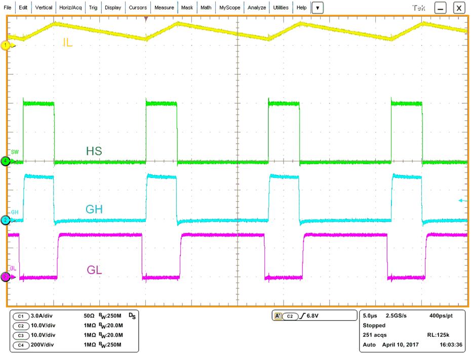
 Refer to Figure 47 below for the UCC27712 driving 40-A, 650-V IGBT's in a high voltage sync buck configuration. The input voltage is 400 V, output 100 V with a 150-W output load. Channel 1 is the inductor current, Channel 2 is high-side IGBT VGE, Channel 3 is low-side IGBT VGE, and Channel 4 is the switch node or HS voltage.
 Figure 47. IGBT Sync-Buck Operating at 400 V and 150 W