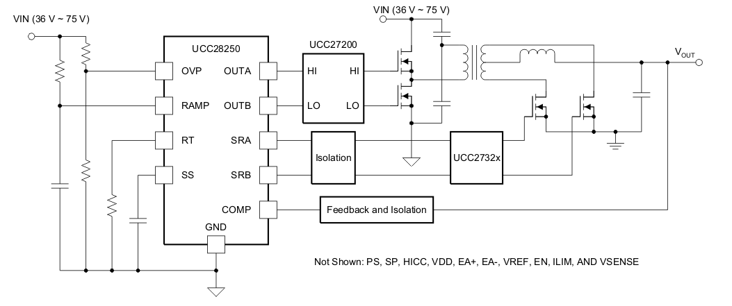
The UCC28250 PWM controller is designed for high power density applications that may have stringent prebiased start-up requirements. The integrated synchronous rectifier control outputs target high-efficiency and high-performance topologies such as half-bridge, full-bridge, interleaved forward, and push-pull. The UCC27200 half-bridge drivers and UCC2732X MOSFET drivers used in conjunction with the UCC28250 provide a complete power converter solution.
Externally programmable soft-start, used in conjunction with an internal prebiased start-up circuit, allows the controller to gradually reach a steady-state operating point under all output conditions. The UCC28250 can be configured for primary or secondary-side control and either voltage or current mode control can be implemented.
The oscillator operates at frequencies up to 2 MHz, and can be synchronized to an external clock. Input voltage feedforward, cycle-by-cycle current limit, and a programmable hiccup timer allow the system to stay within a safe operation range. Input voltage, output voltage and temperature protection can be implemented. Dead time between primary-side switch and secondary-side synchronous rectifiers can be independently programmed.
PART NUMBER | PACKAGE | BODY SIZE (NOM) |
---|---|---|
UCC28250 | TSSOP (20) | 6.50 mm × 4.40 mm |
VQFN (20) | 4.00 mm × 3.50 mm |
Changes from C Revision (July 2011) to D Revision
Changes from B Revision (October 2010) to C Revision
Changes from A Revision (April, 2010) to B Revision
PIN | I/O | DESCRIPTION | ||
---|---|---|---|---|
NAME | QFN | PW | ||
COMP | 3 | 10 | I/O | Error amplifier output |
EN | 18 | 5 | I | Device enable and disable |
FB/EA- | 2 | 9 | I | Error amplifier inverting input |
GND | 4 | 11 | I | Ground |
HICC | 10 | 17 | I | Cycle-by-cycle current limit time delay and Hiccup time setting |
ILIM | 17 | 4 | I | Current sense for cycle-by-cycle overcurrent protection |
OUTA | 9 | 16 | O | 0.2-A sink/source primary switching output |
OUTB | 8 | 15 | O | 0.2-A sink/source primary switching output |
OVP/OTP | 19 | 6 | I | Overvoltage and overtemperature protection pin |
PS | 11 | 18 | I | Primary off to synchronous rectifier on dead-time set |
RAMP/CS | 16 | 3 | I | PWM ramp input (for voltage mode control) or current sense input (for current mode control) |
REF/EA+ | 1 | 8 | I | Error amplifier noninverting input |
RT | 15 | 2 | I | Oscillator frequency set or synchronous clock input |
SP | 12 | 19 | I | Synchronous rectifier off to primary on dead-time set |
SRA | 7 | 14 | O | 0.2-A sink/source synchronous rectifier output |
SRB | 6 | 13 | O | 0.2-A sink/source synchronous rectifier output |
SS | 13 | 20 | I/O | Soft-start programming |
VDD | 5 | 12 | I | Bias supply input |
VREF | 20 | 7 | O | 3.3-V reference output |
VSENSE | 14 | 1 | I | Output voltage sensing for prebias control |
MIN | MAX | UNIT | ||
---|---|---|---|---|
VDD(3) | Input supply voltage | –0.3 | 20 | V |
OUTA, OUTB, SRA and SRB | –0.3 | VDD + 0.3 | V | |
COMP | –0.3 | VREF + 0.3 | V | |
Input voltages on SS and EN | –0.3 | 5.5 | V | |
Input voltages on RT, PS, SP, ILIM, OVP, HICC, VSENSE, EA+ and EA- | –0.3 | 3.6 | V | |
Input voltage on RAMP/CS | –0.3 | 4.3 | V | |
Output voltage on VREF | –0.3 | 3.6 | V | |
Lead temperature (soldering 10 sec) PW package | 300 | °C | ||
Tstg | Storage temperature | –65 | 150 | °C |
VALUE | UNIT | |||
---|---|---|---|---|
V(ESD) | Electrostatic discharge | Human-body model (HBM), per ANSI/ESDA/JEDEC JS-001(1) | ±3000 | V |
Charged-device model (CDM), per JEDEC specification JESD22-C101(2) | ±2000 |
THERMAL METRIC | UCC28250 | UNIT | ||
---|---|---|---|---|
RGB (VQFN) | PW (TSSOP) | |||
20 PINS | 20 PINS | |||
RθJA | Junction-to-ambient thermal resistance | 126 with hot spot, 104 without hot spot |
60.3 with hot spot, 39.3 without hot spot |
°C/W |
RθJC(top) | Junction-to-case(top) thermal resistance | 31.5 | °C/W | |
RθJB | Junction-to-board thermal resistance | 55.8 | °C/W | |
RθJC(bot) | Junction-to-case(bottom) thermal resistance | 0.8 | °C/W |
PARAMETER | TEST CONDITIONS | MIN | TYP | MAX | UNIT | |
---|---|---|---|---|---|---|
SUPPLY CURRENTS | ||||||
IDD(off) | Start-up current | VDD = 3.6 V | 150 | 275 | µA | |
IDD | Operating supply current | 100-pF capacitor on OUTA, OUTB, SRA and SRB | 2 | 2.7 | 3.4 | mA |
IDD(dis) | Standby current | EN = 0 V | 250 | 425 | 600 | µA |
UNDERVOLTAGE LOCKOUT | ||||||
VUVLOR | Start threshold | 4 | 4.3 | 4.6 | V | |
VUVLOF | Minimum operating voltage after start | 3.8 | 4.1 | 4.4 | V | |
Hysteresis | 0.15 | 0.2 | 0.25 | V | ||
SOFT START | ||||||
ISS | Soft-start charge current | VSS = 0 V | 25 | 27 | 29 | µA |
VSS(max) | Clamp voltage | 3.3 | 3.6 | 4 | V | |
ENABLE(2) | ||||||
Trigger threshold | 2.25 | V | ||||
Minimum pulse width for pulse enable | 3 | µs | ||||
ERROR AMPLIFIER | ||||||
High-level COMP voltage | 2.8 | 3 | V | |||
Low-level COMP voltage | 0.3 | 0.4 | V | |||
Input offset | -12 | 12 | mV | |||
Open loop gain | 70 | 100 | dB | |||
ICOMP(snk) | COMP sink current | 3 | 6.5 | 9 | mA | |
ICOMP(src) | COMP source current | 2 | 4.5 | 8 | mA | |
OSCILLATOR | ||||||
FSW(nom) | Nominal switching frequency at OUTA or OUTB set by RT resistor | RT/SYNC = 75 kΩ, RSP = 20 kΩ | 185 | 200 | 215 | kHz |
FSW(min_sync) | Minimum switching frequency at OUTA or OUTB set by external sync frequency | fRT/SYNC = 100 kHz | 85 | kHz | ||
FSW(max_sync) | Maximum switching frequency at OUTA or OUTB set by external sync frequency | fRT/SYNC = 2.5 MHz | 1.15 | MHz | ||
External synchronization signal high | 1 | V | ||||
External synchronization signal low | 0.2 | V | ||||
VOLTAGE REFERENCE | ||||||
VVREF | Output voltage | VDD = from 7 V to 17 V, IVREF = 2 mA | 3.22 | 3.3 | 3.38 | V |
0 < IREF < 10 mA | 3.22 | 3.3 | 3.38 | |||
Short circuit current | VREF = 3 V, TJ = 25°C | 12 | 25 | 40 | mA | |
CURRENT SENSE, CYCLE-BY-CYCLE CURRENT LIMIT WITH HICCUP | ||||||
VILIM | ILIM cycle-by-cycle threshold | 0.495 | 0.502 | 0.509 | V | |
TPDILIM | Propagation delay from ILIM to OUTA and OUTB outputs | Exclude leading edge blanking | 15 | 25 | 36 | ns |
TBLANK | leading edge blanking | 40 | 60 | 90 | ns | |
Current limit shutdown delay timing program current | Measured at HICC pin | 55 | 75 | 95 | µA | |
Hiccup timing program current | Measured at HICC pin | 2 | 2.7 | 3.5 | µA | |
VHICC_SD | Current limit shutdown delay timer threshold at HICC | 0.55 | 0.6 | 0.65 | V | |
VHICC_PU | HICC pullup threshold | 2.3 | 2.4 | 2.5 | V | |
VHICC_RST | Hiccup restart threshold | 0.25 | 0.3 | 0.35 | V | |
VCS(max) | RAMP/CS clamp voltage | 10-V ramp charging voltage source with 40-kΩ current limiting resistor | 3.5 | 4 | 4.5 | V |
OVP/OTP COMPARATOR | ||||||
VOVP | Internal reference | 0.66 | 0.7 | 0.74 | V | |
IOVP | Internal current | 8.5 | 11 | 13.5 | µA | |
PRIMARY OUTPUTS | ||||||
Rise/fall time | CLOAD = 100 pF | 8 | ns | |||
RSRC | Output source resistance | IOUT = 20 mA | 12 | 20 | 35 | Ω |
RSNK | Output sink resistance | IOUT = 20 mA | 4 | 12 | 30 | Ω |
SYNCHRONOUS RECTIFIER OUTPUTS | ||||||
Rise/fall time | CLOAD = 100 pF | 8 | ns | |||
RSRC | Output source resistance | IOUT = 20 mA, VDD = 12 V | 12 | 20 | 35 | Ω |
IOUT = 20 mA, VDD = 5 V | 15 | 25 | 45 | |||
RSNK | Output sink resistance | IOUT = 20 mA, VDD = 12 V | 4 | 12 | 30 | Ω |
TDPS | Primary off to secondary on dead time | PS = VREF | -5 | 0 | 7.5 | ns |
PS = 27 kΩ | 27 | 40 | 50 | |||
PS = 27 kΩ, 25°C | 37 | 40 | 43 | |||
TDSP | Secondary off to primary on dead time | SP = VREF | -5 | 0 | 7.5 | ns |
SP = 20 kΩ | 30 | 40 | 50 | |||
SP = 20 kΩ, 25°C | 37 | 40 | 43 |
The UCC28250 is a high-performance PWM controller with advanced synchronous rectifier outputs and is ideally suited for regulated half-bridge, full-bridge and push-pull converters. A dedicated internal prebiased start-up control loop working in conjunction with a primary-side voltage loop achieves prebiased start-up for either primary-side or secondary-side control applications. The UCC28250 architecture allows either voltage mode or current mode control.
Input voltage feedforward can be implemented, allowing PWM ramp generator to improve the converter line transient response. Advanced cycle-by-cycle current limit achieves volt-second balancing even during fault conditions. The hiccup timer helps the system to stay within a safe operation range under over load conditions. With a multifunction OVP/OTP pin, combinations of input voltage protection, output voltage protection and overtemperature protection can be implemented. The UCC28250 allows individual programming of dead time between primary-side switch and secondary-side SRs, to allow optimal power stage design. Dead time can also be reduced to zero, and this allows optimal system configuration considering the delays on the gate driver stage. The UCC28250 also provides complete system level protection functions, including UVLO, thermal shut down and overvoltage, overcurrent protection.
The UCC28250 can be powered up by a wide supply range from 4.3 V (UVLO rising typical) to 20 V (absolute maximum), making it suitable for primary-side control or secondary-side control. When the voltage at the VDD pin is lower than 4.1 V (typical), the controller is in stand-by mode and consumes 150 µA (typical) at 3.6 V VDD. In stand-by mode, VREF continues to be regulated to 3.3 V or follows VDD if VDD is lower than 3.3 V. Refer to the VREF description VREF (Reference Generator) (20/7) for more detailed information. A minimum 1-µF bypass capacitor is required from VDD to ground. Keep the bypass capacitor as close to the device as possible.
The VREF pin is regulated at 3.3 V. An external ceramic capacitor must be placed as close as possible to the VREF and GND pins for noise filtering and to provide compensation to the regulator. The capacitance range must be limited from 0.5 µF to 2 µF for stability. This reference is used to power the controller’s internal circuits, and can also be used to bias an opto-coupler transistor, an external house-keeping microcontroller, or other peripheral circuits. This reference can also be used to generate the reference for an external error amplifier. This regulator output is internally current limited to 25 mA (typical).
The following conditions must be met before the controller allows start-up:
If all these conditions are met, the signal driving the EN pin is able to initiate the soft start process. When the device is enabled, the 27-µA internal charging current at the SS pin is turned on and begins to charge the soft-start capacitor. The EN pin can accept both level-enable and pulse-enable signals.
For level-enable, the voltage level on the EN pin must be continuously higher than 2.25 V to allow continuous operation. When the EN pin falls below 2.25 V, the device is disabled (see Figure 21).
A pulse signal may also be applied to the EN pin. Pulse-enable operation is shown on Figure 22. As long as the EN falling edge happens before the SS voltage reaches 0.3 V, the enable signal at EN pin is considered as a pulse. In this case, the next rising edge at EN pin disables the controller. As long as the falling edge of the first pulse at EN pin happens after SS rises to 0.3 V, the UCC28250 interprets the pulse enable as a level enable, and an external solution as shown on Figure 23 (a) can be used to reduce the pulse width. In this circuit, R2 is used to limit the current (especially the negative current) through the internal ESD cell. Figure 23 (b) illustrates the waveforms based on this solution. To prevent false trigger by noises, the pulse at the EN pin must be at least 2.25 V (minimum) high and 3 µs wide to be considered valid.
Choose the R1, R2, and C values based on the following equations:
Choose R2 based on the current limit requirement from the device.
Choose R1 arbitrarily but much smaller than R2 and choose C1 according to the time constant requirement to generate longer than 3-µs pulse.
In the case that the UCC28250 is enabled with a level EN signal and the SS is discharged internally when the OCP is triggered, pulling the EN pin down before SS rises to 0.3 V cannot disable the part because the controller interprets it to be a pulse enable. In this case, the next rising edge at the EN pin disables the controller. If the designer wants to disable UCC28250 with a level signal during an over current condition, the recommended solution is to pull down the SS pin rather than the EN pin. If the enable function is not used, pull the EN pin to the VREF pin.
The UCC28250 oscillator frequency is set by an external resistor connected between the RT pin and ground. Switching frequency selection is a trade-off between efficiency and component size. Based on the selected switching frequency, the programming resistor value can be calculated as:
In this equation, fSW is the switching frequency and TD(sp) is the dead time between synchronous rectifier turnoff to primary switch turnon. TD(sp) is set by an external resistor between the SP pin and ground (refer to SP (Synchronous Rectifier Turnoff to Primary Output Turnon Dead Time Programming) (13/19)).
Each output (OUTA, OUTB, SRA, SRB) switches at half the oscillator frequency (fSW = ½ x fOSC). Figure 24 shows the relationship between RT and fOSC at certain TD(sp) and can be used to program oscillator frequency accordingly.
The UCC28250 can be synchronized to an external clock by applying an external clock source to the RT pin. Synchronization helps with parallel operation and/or preventing beat frequency noise. The UCC28250 synchronizes its internal oscillator to an external frequency source ranging from 170 kHz to 2.3 MHz, which is equivalent to an 85-kHz to 1.15-MHz switching frequency. The internal oscillator frequency is clamped to 170 kHz during synchronization if the external source frequency drops below 170 kHz.
The UCC28250 aligns the turnon of primary outputs OUTA and OUTB to the falling edge of the synchronizing signal, as shown in Figure 25. If the frequency source is from the gate outputs of another half bridge controller, interleaving can be achieved. The interleaving angle is determined by the frequency source’s duty cycle. When a 50% duty cycle is applied, optimal interleaving is achieved, and EMI filters can be minimized.
The dead time TD(sp) between synchronous rectifier turnoff to primary output turnon is programmed by an external resistor, RSP, connected between the SP pin and ground. The value of RSP can be determined by Figure 27. Zero dead time can be achieved by tying the SP pin to VREF. The falling edge of synchronous rectifier SRA/SRB is aligned with the raising edge of the primary output OUTA/OUTB.
NOTE
The minimum value for RPS/RSP is 5 kΩ and the maximum value is 250 kΩ.
The dead time TD(ps) between primary output turnoff to synchronous rectifier turnon is set by external resistor, RPS, connected between PS pin and ground. The value of is RPS is defined by Figure 28. Zero dead time can be achieved by tying the SP pin to VREF.
NOTE
The minimum value for RPS/RSP is 5 kΩ and the maximum value is 250 kΩ.
The UCC28250 can be controlled using either voltage mode or current mode. RAMP/CS is a multi-function pin used either to generate the ramp signal for voltage mode control or to sense current for current mode control.The following sections describe the RAMP/CS functionality for voltage mode and current mode control.
For voltage mode control, a resistor RCS and a capacitor CCS must be connected to the RAMP/CS pin as shown in Figure 29. The internal pulldown switch has approximately 40-Ω on-resistance. The RAMP/CS pin is clamped internally to 4 V for internal device protection. The CCS value must be small enough to discharge the RAMP/CS pin from its peak voltage to ground within the pulse width of the BLANK signal (TD(sp) + 70 ns). The following formula derives a CCS value.
A CCS value less than 650 pF works for most applications. To minimize the impacts of parasitic capacitance caused by the PCB layout and routing, a minimum of 100 pF is recommended for CCS. Once CCS is determined, RCS can be calculated according to the desired ramp peak amplitude.
In this equation, the VCHARGE is the voltage used to generate the ramp, VPK is the desired ramp amplitude and the fSW is the switching frequency.
Choose the ramp amplitude to accommodate the voltage range of the COMP pin and the maximum duty cycle required by the power stage. Use the following equation to select VPK, in the equation, DMAX is the maximum duty cycle for primary outputs.
Voltage feed-forward can be achieved by driving RCS from line input VIN. The peak of RAMP/CS is proportional to VIN and output has have much faster line transient response. When the UCC28250 is used for the primary-side control, RAMP parameters are critical for the optimal prebiased start-up performance. Refer to the RAMP: Voltage Mode Control With Feed-Forward Operation for a detailed design procedure of choosing RCS.
If the line input cannot be easily accessed due to limited board area or other limitation, a RAMP signal with fixed peak voltage can be implemented by simply driving RCS from 3.3-V VREF (Figure 29).
For current mode control, the RAMP/CS pin is driven by a signal representative of the transformer primary-side current. The current signal must have compatible input range of the COMP pin. As shown in Figure 30, the COMP pin voltage is used as the reference for peak current. The primary-side signals OUTA and OUTB are turned on by the internal clock signal and turned off when sensed peak current reaches the COMP pin voltage. Choose the current sense transformer turns ratio (1:n) and the burden resistor value (RB) based on the peak current at maximum load IMAX.
REF/EA+ is the noninverting input of the UCC28250’s internal error amplifier.
When the UCC28250 is configured for secondary-side control, the internal error amplifier is used as the control loop error amplifier. Connect REF/EA+ directly to the VREF pin to provide the reference voltage for the feedback loop.
When the UCC28250 is configured for primary-side control, the error amplifier is connected as a voltage follower. Connect REF/EA+ to the opto-coupler output.
The voltage range on REF/EA+ pin is 0 V to 3.7 V.
FB/EA- is the inverting input of the UCC28250’s internal error amplifier.
When the UCC28250 is configured for secondary-side control, connect the output voltage sensing divider to this pin. The voltage divider can be selected according to the voltage on REF/EA+ pin. Referring to Figure 32, pick the lower resistor RO1 value arbitrarily, and choose the upper resistor RO2 value as:
Because the control loop gain is affected by voltage divider resistor values, choose an appropriate RO1 value so that the voltage loop DC gain is larger than 40 dB to prevent interference between the primary-side control loop and the SR control loop during start-up.
When the UCC28250 is sitting on the primary side, the error amplifier is connected as a voltage follower. Connect FB/EA- directly with COMP pin.
The maximum voltage allowed on FB/EA- pin is 3.7 V.
The COMP pin is the internal error amplifier’s output and also the input signal for PWM comparator. The maximum input common voltage of the PWM comparator is 2.8 V. It is suggested to program the peak value of RAMP to be lower than 2.3 V. Otherwise, the voltage of COMP pin should be clamped to be lower than 2.8 V by external circuit to make the internal PWM comparator work properly. Figure 31 shows tan external circuit that is recommended for voltage clamp function. Both the primary-side switches’ duty cycle and secondary-side SRs’ duty cycle is controlled by the COMP pin voltage. At steady state, a higher COMP pin voltage results in a larger duty cycle for the primary-side switches and a smaller duty cycle on the SRs.
When the UCC28250 controller is set up for secondary-side control, connect the compensation network from the FB/EA- pin to the COMP pin.
For primary-side control, the error amplifier is connected as a voltage follower. Directly connect the COMP pin to the FB/EA- pin.
The VSENSE pin is used to directly sense the output voltage and to feed it into a transconductance error amplifier. The measured voltage allows the UCC28250 to achieve optimal prebiased start-up performance.
When configured as a secondary-side controller, the output voltage is sensed and fed into the FB/EA- pin. The UCC28250 uses a conventional error amplifier approach to allow type III compensation. Therefore, the FB/EA- pin voltage always follows the REF/EA+ voltage. The FB/EA- pin does not reflect the true output voltage and therefore this dedicated VSENSE pin is required. The voltage divider connected to VSENSE is discussed in the Prebiased Start-Up Section.
When UCC28250 is set up as primary-side control, connect VSENSE pin to VREF.
The soft-start circuit gradually increases the converter’s output voltage until steady state operation is reached. This reduces start-up stresses and current surge.
When the UCC28250 reaches its valid operating threshold, the SS pin capacitor is charged with a 27-µA current source. The UCC28250’s internal error amplifier noninverting terminal follows the SS pin voltage on REF/EA+ pin voltage depending on which one is lower. Hence, during soft start, the SS pin voltage is lower than REF/EA+. The internal error amplifier then uses the SS pin as its reference voltage, until the SS pin voltage rises above the REF/EA+ level. Once the SS pin voltage is above REF/EA+ voltage, soft-start time is considered finished.
The soft-start implementation scheme and timing is different, depending on the location of the UCC28250 with respect to the isolation barrier.
For secondary-side control, the internal error amplifier is used to achieve the voltage regulation. The REF/EA+ is connected to an external reference voltage, FB/EA- is connected to the voltage sensing divider, and the error amplifier’s output pin (COMP) is connected through a compensation filter back to the FB/EA- pin (Figure 32). In this case, the primary output’s start-up is a closed loop soft start (soft-start input reference of error amplifier). The output soft-start time is determined by the external capacitor connected at SS pin based on the internal 27-µA charging current and the voltage set at REF/EA+ pin.
Based on the soft-start time TSS, choose soft start capacitor CSS value as:
For primary-side control, the internal error amplifier is connected as a buffer stage. In other words, the COMP pin is shorted to the FB/EA- pin, and the output of an external error amplifier is connected to the REF/EA+ pin through an optical coupler (Figure 33). In this case, the output start-up is an open loop soft start because the COMP follows the soft-start voltage instead of the voltage loop output. The soft-start time is still determined by external capacitor CSS and the 27-µA internal charge current. The voltage depends on the value of final COMP voltage which corresponds to the regulated primary output duty cycle. According to the desired soft start time and COMP pin voltage level at steady state, the SS pin capacitor can be calculated as:
After soft start, the voltage at SS pin is eventually clamped at around 4 V. Under fault conditions (UVLO, internal thermal shut down, OVP/OTP, hiccup mode), or when externally disabled, SS pin is pulled down to ground quickly by an internal switch with 2 kΩ on resistance to prepare for re-start. Pulling SS pin to ground externally shuts down the controller as well.
Cycle-by-cycle current limit is accomplished using the ILIM pin for current mode control or for voltage mode control. The input to the ILIM pin represents the primary current information. If the voltage sensed at ILIM pin exceeds 0.5 V, the current sense comparator terminates the pulse of output OUTA or OUTB. If the high current condition persists, the controller operates in a cycle-by-cycle current limit mode with duty cycle determined by the current sense comparator instead of the PWM comparator. ILIM pin is pulled down by an internal switch at the rising edge of every clock cycle. This internal switch remains on for an additional 70 ns after OUTA or OUTB goes high to blank leading edge transient noise in the current sensing loop. This reduces the filtering requirements at the ILIM pin and improves the current sense response time.
Once the over current protection level IPK is selected, the current transformer turns ratio and the burden resistor value can be decided as:
In this equation, current transformer turns ratio is 1:n and RS is the burden resistor value.
Some filtering capacitance is required to reduce the sensing noise. Choose the RC constant at about 100 ns, and calculate the capacitor value as:
The cycle-by-cycle current limit operation time before all four outputs shut down can be programmed by external capacitor CHICC at HICC pin. (See HICC pin description)
The cycle-by-cycle current limit operation time before all four outputs shut down can be programmed by an external capacitor CHICC from HICC pin to ground, as shown in Figure 34. Once all four outputs are shutdown, controller goes into hiccup cycle which is about 100 times of the cycle-by-cycle current limit shut-down delay time. A 1-mA internal current source charges HICC pin up to 2.4 V, then the HICC pin is discharged by a 2.7-µA internal current source to generate long hiccup restart time until HICC reaches 0.3 V. Based on the system requirement, once the cycle-by-cycle current limit delay time TOC(delay) is selected, the HICC pin capacitor CHICC can be selected based on the equation
As shown in Figure 35, cycle-by-cycle current limiting shut-down delay time is:
And hiccup-restart-time THICC is equal to:
As soon as the outputs are shut-down, the SS pin is pulled to ground internally until the hiccup restart timer is reset after time duration THICC.
The OVP/OTP pin provides multiple fault protection functions. If the voltage on the OVP/OTP pin exceeds 0.7 V, a fault shutdown occurs. All outputs stop switching and stay off (low) during the shutdown, and the SS pin is pulled to ground internally. Once the fault condition is cleared (that is, OVP/OTP voltage drops below 0.7 V), the UCC28250 enters hiccup mode. A soft-start cycle begins after the hiccup cycle is finished. An internal 11-µA switched current source is used to create hysteresis.
If the external resistor divider runs from line voltage VIN, a line overvoltage protection is implemented.
If the external resistor divider runs from the output voltage, output overvoltage fault protection is achieved. Figure 36 shows the overvoltage protection external configuration at the OVP/OTP pin.
According to the protection threshold VR and recovery threshold VF, choose an arbitrary R2 value. To ensure a realistic solution, R2 must meet the following:
The other two resistors, R1 and R3 can be calculated.
If the external resistor divider runs from 3.3-V VREF, and replaces R2 with a positive temperature coefficient (PTC) thermistor, an overtemperature fault protection with programmable hysteresis is accomplished (Figure 37). Choose an arbitrary PTC value, which has a resistance as RPTC1 at protection temperature and resistance as RPTC2 at recovery temperature. Because of its positive temperature coefficient, RPTC1 is larger than RPTC2. To ensure an available solution, RPTC1 and RPTC2 need to meet the criteria.
And resistors R1 and R3 can be calculated as:
Figure 38 shows an external configuration using the OVP/OTP pin to achieve both overvoltage and overtemperature protection. Follow the same design procedure for the OVP setting to choose R1, R2, and R3. Choose an NTC value at protection temperature much smaller than R1 and with the resistance at protection temperature as RNTC1, and recover temperature as RNTC2. The R4 value can be calculated as:
Because of the interaction between the two voltage dividers, overtemperature protection thresholds move slightly with the different input voltages.
OUTA and OUTB are the primary-side switch control signals. With the 0.2-A peak current capability, an external gate driver is required.
SRA and SRB are the synchronous rectifier control signals. With the 0.2-A peak current capability, an external gate driver is required.
GND pin is the ground reference for the whole device. Tie all the signal returns to this pin.
The UCC28250 can be controlled using either voltage mode or current mode. RAMP/CS is a multi-function pin used either to generate the ramp signal for voltage mode control or to sense current for current mode control. Refer to RAMP/CS (PWM Ramp Input or Current Sense Input) (16/3) for the details.
NOTE
Information in the following applications sections is not part of the TI component specification, and TI does not warrant its accuracy or completeness. TI’s customers are responsible for determining suitability of components for their purposes. Customers should validate and test their design implementation to confirm system functionality.
The UCC28250 is a high-performance PWM controller with advanced synchronous rectifier outputs and is ideally suited for regulated half-bridge, full-bridge and push-pull converters. A dedicated internal prebiased start-up control loop working in conjunction with a primary-side voltage loop achieves monotonic prebiased start-up for either primary-side or secondary-side control applications. The UCC28250 architecture allows either voltage mode or current mode control.
Input voltage feedforward can be implemented, allowing PWM ramp generator to improve the converter line transient response. Advanced cycle-by-cycle current limit achieves volt-second balancing even during fault conditions. The hiccup timer helps the system to stay within a safe operation range under over load conditions. With a multifunction OVP/OTP pin, combinations of input voltage protection, output voltage protection and overtemperature protection can be implemented. The UCC28250 allows individual programming of dead time between primary-side switch and secondary-side SRs, To allow optimal power stage design. Dead time can also be reduced to zero, and this allows optimal system configuration considering the delays on the gate driver stage. The UCC28250 also provides complete system level protection functions, including UVLO, thermal shut down and overvoltage, overcurrent protection.
The UCC28250 includes a high-performance internal error amplifier with low input offset, high source/sink current capability and high gain bandwidth (typical 3.5 MHz). The reference of the error amplifier (REF/EA+ pin) is set externally to support flexible trimming of the voltage loop, and to make the controller flexible for both primary side, as well as secondary-side control. The extra positive input for the error amplifier is the SS pin which is used to externally program the soft-start time of the converter’s output.
During steady state operation, the primary switch duty cycle, D, is generated based on the external ramp on RAMP/CS pin and the COMP pin voltage. A higher COMP pin voltage results in a larger duty cycle. The secondary-side SR duty cycle is SR_D = (1-D), complementary to the primary-side duty cycle, without considering the dead time between primary-side switch and secondary-side SR. The primary outputs begin to switch when COMP pin voltage is above the 350 mV internal offset. The synchronous rectifier outputs only switch after COMP pin voltage is above 550 mV internal offset. According to the internal logic, the minimum pulse width for the primary-side OUTA and OUTB is typically 100 ns.
During soft start, the primary-side switch duty cycle is generated based on the external ramp on RAMP/CS pin and the COMP pin voltage. However, the duty cycle of secondary-side SR is generated based on an internal ramp and the COMP pin voltage. When the converter is controlled on the primary side, an internal ramp is a fixed ramp with 3-V peak voltage. When the converter is controlled on secondary side, an internal ramp is generated based on the internal prebiased start-up loop. An internal prebiased start-up loop modifies the SR duty cycle during soft start to achieve the optimal prebiased start-up performance.
After the SS pin reaches 2.9 V, the prebiased start-up control loop is disabled. The secondary-side SR instantaneously changes into its steady state value as complementary to the primary-side duty cycle.
With the internal error amplifier, UCC28250 supports both primary-side control and secondary-side control. For different control methods, the controller is configured accordingly and so is the prebiased start-up control. During soft start, both the primary-side switches’ duty cycle and secondary-side SRs’ duty cycle are increased. This gradually increases the output voltage until steady state operation is reached, thereby reducing surge current.
For secondary-side control, the UCC28250 implements close-loop control of both the primary-side switches and secondary-side synchronous rectifiers’ duty cycles. This makes it easy to achieve optimal start-up performance.
The internal error amplifier is set up as the control loop error amplifier. Connect REF/EA+, FB/EA-, COMP and VSENSE as shown in Figure 39. To achieve optimal prebiased start-up performance, the output voltage must be directly measured. The UCC28250 uses the VSENSE pin to directly sense this output voltage. Choose the voltage dividers on VSENSE slightly different to the FB/EA- voltage divider so that the voltage on VSENSE pin is roughly 10% to 15% more than FB/EA- pin voltages. Select RO1 equal to RS1, and RS2 about 10% to 15% smaller than RO2.
The error amplifier uses the lower voltage between the SS pin and the REF/EA+ pin to be the reference voltage for the feedback loop. In this method, the control loop is said to be ‘closed’ during the entire start-up process, as it is always based on the true output voltage.
During soft start, the primary-side switch duty cycle is controlled by the COMP pin voltage and ramp voltage generated on the RAMP/CS pin. A higher COMP pin voltage results in larger duty cycle. However, to improve start-up performance, the secondary-side synchronous rectifier duty cycle is controlled by a separate, internal ramp signal (generated by a dedicated prebiased start-up loop) and by the COMP pin voltage. This dedicated prebiased loop is much faster than the regular voltage loop to avoid interaction between the two loops. The start-up loop reads the output voltage through a transconductance error amplifier connected to the VSENSE pin. When the output voltage is higher than the reference, the prebiased start-up loop increases the SR duty cycle to reduce the output voltage. Conversely, when the output voltage is lower than the reference, the SR duty cycle is decreased to help maintain higher output voltage. To speed up the start-up time, the minimum duty cycle of the synchronous rectifier is 50%.
Once the soft start is finished, the prebiased loop is disabled and the duty cycle of the synchronous rectifiers becomes the complimentary of primary switches’ duty cycle, with some dead time inserted in between.
When the UCC28250 is sitting on the primary side, the internal error amplifier is connected as a voltage follower and an extra error amplifier is needed on the secondary side for closed loop control. The error amplifier implementation is shown in Figure 40.
In the above configuration, the UCC28250 can only see the control loop feedback voltage, and cannot directly access the output voltage. The design of the soft-start time is critical to achieve optimal prebiased start-up performance. Some trial and error approaches are needed to achieve optimal performance. It is also important to choose the appropriate ramp amplitude. Refer to RAMP/CS (PWM Ramp Input or Current Sense Input) (16/3) discussion on the detailed design procedure for choosing ramp generation components.
During soft start, regardless of the prebiased condition, the output voltage is always lower than the regulation voltage, so that the feedback loop is always saturated. When the internal error amplifier is connected as a voltage follower, the COMP voltage follows the lower of the voltage on the RER/EA+ pin and the SS pin. Because the feedback loop is saturated, the COMP pin always follows the SS pin voltage, until the output voltage becomes regulated and the feedback voltage takes over. In this control method, the output voltage control loop is always saturated, and the controller soft starts the COMP pin voltage. Therefore, it is called open loop soft start.
The primary-side switch duty cycle is controlled by the COMP pin voltage and by the RAMP/CS pin voltage. During soft start, the COMP pin voltage follows the SS pin as it is rising, so the primary-side switch duty cycle keeps increasing. When the output voltage becomes regulated, the feedback voltage becomes less than the SS pin voltage and the primary-side switch comes controlled by the control loop.
For the primary-side control setup, because output voltage is not directly accessible, the internal prebiased start-up loop is disabled by connecting VSENSE to VREF. Instead, the internal ramp used to generate the synchronous rectifier duty cycle is fixed, with the peak voltage of 3 V. The duty cycle of the synchronous rectifier increases as the SS pin voltage increases. When the SS pin voltage reaches 2.9 V, the soft start is considered finished and the synchronous rectifier duty cycle becomes the complementary of the primary-side switch duty cycle, minus the programmed dead time. Because of different COMP pin voltages at different line voltages, the SR duty cycle generated by the internal ramp might be different than the complementary of the primary-side switch duty cycle (1-D). If the duty cycle is too large, the internal logic is able to limit the duty cycle to (1-D). However, if the duty cycle is too small, when the soft start is finished, the SR duty cycle has a sudden change, which will cause output voltage disturbance. To optimize the prebiased start-up performance, TI recommends that the duty cycle change at the end of soft start be as small as possible.
For voltage mode control, a resistor RCS and a capacitor CCS are connected externally at RAMP/CS pin as shown in Figure 41. A ramp signal is generated on the RAMP/CS pin, at a rate of two times that of the switching frequency. The generated ramp signal is used to control the duty cycle for both the primary-side switches and secondary-side synchronous rectifiers. The ramp amplitude can be fixed or variable with the input voltage (input voltage feedforward).
To realize a fixed amplitude ramp, connect RCS to the VREF pin, so that the ramp capacitor charging voltage is fixed regardless of line and load condition. The RAMP/CS pin is clamped internally to 4 V for internal device protection. Because the internal pulldown switch has about 40-Ω on-resistance, the CCS value must be small enough to discharge RAMP/CS from the peak to ground within TD(sp) + 70 ns (that is, the pulse width of BLANK signal).
To achieve the input voltage feedforward, the slope of the ramp must be proportional to the input voltage. Tie RCS to the input line voltage. Because the ramp voltage is much lower than the input voltage, the ramp capacitor charging current is considered to be proportional to the input voltage. With input voltage feedforward, the COMP pin voltage should only move slightly even with large input voltage variation. This will provide much better line transient response for the converter.
The input voltage feedforward also helps on prebiased start-up. When doing primary-side control to prebiased start-up, three conditions need to be considered:
At initial start-up, the primary side must provide enough energy to prevent output voltage dip;
At the end of soft start, it is required to keep the SR duty cycle change to be as small as possible. With input voltage feedforward, the COMP pin voltage is virtually fixed for different input voltages. Therefore, before the end of soft start, the duty cycle is the same for different input voltages. Choose the RCS and CCS following the procedure.
Considering initial start-up, the RAMP peak voltage should be:
In this equation, VIN is the input voltage because of the feedforward any input voltage should be fine; VPRE-BIAS is the highest prebias start-up voltage required by the system; n is the tranformer primary to secondary turns ratio and VSR(ramp) is the internal SR ramp peak voltage 3 V.
Another consideration is at the end of soft start, the SR duty cycle changes from controlled by the soft start, to complimentary to the primary-side duty cycle. The design should keep the transition as smooth as possible. Considering this, based on the output voltage and input voltage range, as well as the transformer turns ratio, calculate the SR duty cycle at different line voltages.
Next, based on the maximum duty cycle on the SR_DMAX, and the internal fixed ramp amplitude 3 V, the COMP voltage at regulation can be chosen as:
Use the calculated COMP pin voltage to derive the external ramp amplitude
According to the calculated ramp voltage from Equation 23 and Equation 25 some trade off is required to pick up the appropriate ramp voltage. Based on the selected ramp capacitor CCS value, choose the ramp resistor RCS value:
In this equation, VIN(max) is the maximum input voltage, fSW is the switching frequency.
Because these calculations ignore the dead time and the non-linearity of the ramp, slight modification is expected to achieve the optimal design. When the input voltage feed forward is not used, refer to RAMP/CS (PWM Ramp Input or Current Sense Input) (16/3) for RC calculation.
For peak current mode control, RAMP/CS pin is connected directly with the current signal generated from a current transformer. The current signal must be compatible with the input range of the COMP pin. External slope compensation is required to prevent sub-harmonic oscillation and to maintain flux-balance. The slope compensation can be implemented by using OUTA and OUTB to charge external capacitors and use the voltage follower to add into the sensed the current signal, as shown in Figure 42. Follow the peak current mode control theory to select compensation slope or refer to Modeling, Analysis and Compensation of the Current-Mode Converter, (SLUA101).
Cycle-by-cycle current limit is accomplished using the ILIM pin for both current mode control and voltage mode control. The input to the ILIM pin represents the primary current information. If the voltage sensed at ILIM pin exceeds 0.5 V, the current sense comparator terminates the pulse of output OUTA or OUTB. If the high current condition persists, the controller operates in a cycle-by-cycle current limit mode with duty cycle determined by the current sense comparator instead of the PWM comparator. ILIM pin is pulled down by an internal switch at the rising edge of each clock cycle. This internal switch remains on for an additional 70 ns after OUTA or OUTB goes high to blank leading edge transient noise in the current sensing loop. This reduces the filtering requirements at the ILIM pin and improves the current sense response time.
UCC28250 makes it possible to maintain flux balance during cycle-by-cycle current limit operation. The duty cycles of primary switches are always matched. If one switch duty cycle is terminated earlier because of current limiting, a matched duty cycle is applied to the other switch for the next half switching cycle, regardless of the current condition, as shown in Figure 43. This matched duty cycle helps to maintain volt-second balancing on the transformer and prevents the transformer saturation.
Once the current limit is triggered, the 75-µA internal current source begins to charge the capacitor on HICC pin. If the current limit condition went away before HICC pin reaches 0.6 V, the device stops charge HICC capacitor and begins to discharge it with 2.7-µA current source. If the cycle-by-cycle current limit condition continues, HICC pin reachs 0.6 V, and all four outputs are shut down. The UCC28250 then enters hiccup mode. During hiccup mode, all four outputs keep low; SS pin is pulled to ground internally; a 2.7-µA current source continuously discharge HICC pin capacitor; until HICC pin voltage reaches 0.3 V. After that, HICC pin is discharged internally to get ready for the next HICC event. The whole converter starts with soft start after hiccup mode.
The cycle-by-cycle current limit operation time before all four outputs shut down is programmed by external capacitor CHICC at HICC pin. The delay time can be calculated as:
The hiccup timer keeps all outputs being zero until the timer expires. The hiccup time THICC is calculated as:
As soon as the outputs are shut-down, SS pin is pulled down internally until the hiccup restart timer is reset after time duration THICC. The detailed illustration of HICCUP mode is shown in Figure 44.
The example provided shows how to design a symmetrical half bridge converter of voltage mode control with UCC28250 on primary side.
Figure 45 is the circuit diagram to be used in this design example. This design example shows how to determine the values in the circuit associated to UCC28250 programming.
Table 1 shows the specifications for the design example.
PARAMETER | MIN | TYP | MAX | UNIT | |
---|---|---|---|---|---|
VIN | Input voltage | 36 | 48 | 72 | VDC |
VOUT | Output voltage | 3.3 | VDC | ||
POUT | Output power | 75 | W | ||
IOUT | Output load current | 23 | A | ||
COUT | Load capacitance | 5000 | µF | ||
fSW | Switching frequency | 150 | kHz | ||
PLIMIT | Over-power limit | 150% | |||
η | Efficiancy at full load | 90% | |||
Isolation | 1500 | V |
The power stage design in this example is standard and the same as that for symmetrical half bridge converter of voltage mode control. From the standard design, these components are determined. This includes Q1 through Q4, C1, C2, CT1, D1 and D2, D3, T1, T2 and T3, and U6. Their design is standard. Also, design associated to current sensing and protection is also standard. This includes CT1, D1, D2, R5 and C5.
D3 (TLV431) with U6, R6, R9, R10, R12, R13, C11 and C12 are composed of standard type 3 feedback loop compensation network and output voltage set point. Their design is also standard.
PARAMETER | MIN | TYP | MAX | UNIT | |
---|---|---|---|---|---|
VIN | Input voltage | 36 | 48 | 72 | VDC |
VOUT | Output voltage | 3.3 | VDC | ||
POUT | Output power | 75 | W | ||
IOUT | Output load current | 23 | A | ||
COUT | Load capacitance | 5000 | µF | ||
fSW | Switching frequency | 150 | kHz | ||
PLIMIT | Over-power limit | 150% | |||
η | Efficiency at full load | 90% | |||
Isolation | 1500 | V |
Equation 3 is used to determine RT based on switching frequency, 300 kHz and assumes the dead time of 150 ns.
There are two-fold considerations to determine RAMP resistance and capacitance. Equation 23 provides RAMP consideration for SR initial start-up with prebias. The corresponding RAMP peak voltage is determined with input voltage low line and maximum prebias output voltage. In the following, T1 turns ratio n = 4.
Equation 24 and Equation 25 provides RAMP consideration for soft start completion to make duty cycle match (1-D) = SR_D.
As different RAMP resistor values are obtained, at this stage, we may take their average value for initial design.
Determine soft-start capacitance with soft-start time 15 ms.
Assuming the dead time is 150 ns, Select R7 = R8 = 121 kΩ based on Figure 27 and Figure 28.
Assuming off time is 0.8 s (Equation 15).
Assuming OV_OFF = 73 V, OV_ON = 72 V (Equation 16 to Equation 18).
As recommended by the data sheet, select C6 = C4 = 1 µF. The final design is shown in Figure 46.
UCC28250 also supports secondary-side control. Refer to Figure 53. In this configuration, the UCC28250 can be used in a design that produces smooth turnon performance with an output prebias condition. The design example and guidelines are summarized in Designing UCC28250 as a Secondary Side Control for Output Turn-On with a Pre-Bias Condition, SLAA477, and Using the UCC28250EVM-564, SLUU441.