SLUSCR9B June 2017 – December 2020 UCC28730-Q1
PRODUCTION DATA
- 1 Features
- 2 Applications
- 3 Description
- 4 Revision History
- 5 Pin Configuration and Functions
- 6 Specifications
-
7 Detailed Description
- 7.1 Overview
- 7.2 Functional Block Diagram
- 7.3 Feature Description
- 7.4 Device Functional Modes
-
8 Application and Implementation
- 8.1 Application Information
- 8.2
Typical Application
- 8.2.1 Design Requirements
- 8.2.2
Detailed Design Procedure
- 8.2.2.1 Stand-By Power Estimate
- 8.2.2.2 Input Bulk Capacitance and Minimum Bulk Voltage
- 8.2.2.3 Transformer Turns Ratio, Inductance, Primary-Peak Current
- 8.2.2.4 Transformer Parameter Verification
- 8.2.2.5 Output Capacitance
- 8.2.2.6 VDD Capacitance, CVDD
- 8.2.2.7 VS Resistor Divider, Line Compensation, and Cable Compensation
- 8.2.2.8 VS Wake-Up Detection
- 8.2.3 Application Curves
- 8.3 Do's and Don'ts
- 9 Power Supply Recommendations
- 10Layout
-
11Device and Documentation Support
- 11.1
Device Support
- 11.1.1
Device Nomenclature
- 11.1.1.1 Capacitance Terms in Farads
- 11.1.1.2 Duty-Cycle Terms
- 11.1.1.3 Frequency Terms in Hertz
- 11.1.1.4 Current Terms in Amperes
- 11.1.1.5 Current and Voltage Scaling Terms
- 11.1.1.6 Transformer Terms
- 11.1.1.7 Power Terms in Watts
- 11.1.1.8 Resistance Terms in Ω
- 11.1.1.9 Timing Terms in Seconds
- 11.1.1.10 DC Voltage Terms in Volts
- 11.1.1.11 AC Voltage Terms in Volts
- 11.1.1.12 Efficiency Terms
- 11.1.1
Device Nomenclature
- 11.2 Documentation Support
- 11.3 Receiving Notification of Documentation Updates
- 11.4 Support Resources
- 11.5 Trademarks
- 11.6 Electrostatic Discharge Caution
- 11.7 Glossary
- 11.1
Device Support
- 12Mechanical, Packaging, and Orderable Information
Package Options
Mechanical Data (Package|Pins)
- D|7
Thermal pad, mechanical data (Package|Pins)
Orderable Information
3 Description
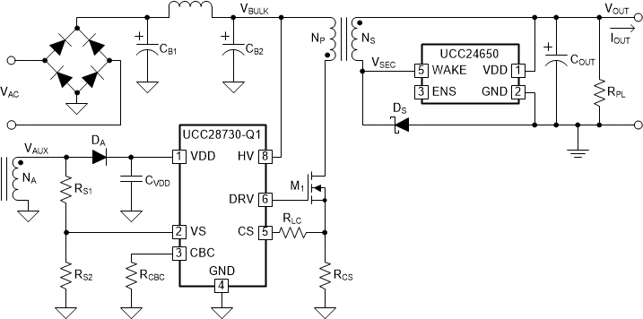
The UCC28730-Q1 isolated-flyback power supply controller provides constant-voltage (CV) and constant-current (CC) output regulation without the use of an optical coupler. A minimum switching frequency of 30 Hz achieves less than 5 mW of no-load power.
This device processes information from the primary power switch and an auxiliary flyback winding for precise control of output voltage and current.
An internal 700-V start-up switch, dynamically- controlled operating states and a tailored modulation profile support ultra-low stand-by power without sacrificing start-up time or output transient response. Control algorithms in the UCC28730-Q1 allow operating efficiencies to meet or exceed applicable standards. Discontinuous conduction mode (DCM) operation with valley-switching reduces switching losses. Modulation of the switching frequency and primary current peak amplitude (FM and AM) keeps the conversion efficiency high across the entire load and line ranges.
| PART NUMBER(1) | PACKAGE | BODY SIZE (NOM) |
|---|---|---|
| UCC28730-Q1 | SOIC (7) | 4.90 mm x 3.90 mm |
 Simplified Schematic
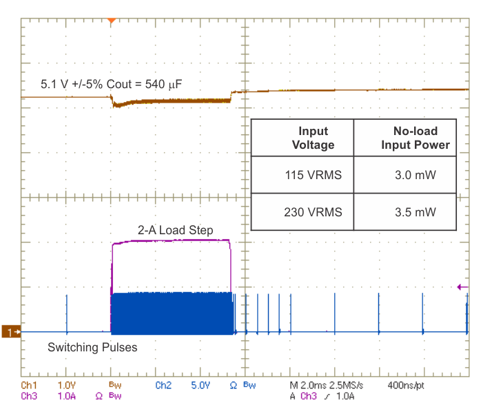
 Zero-Power Input Consumption at
No-Load