SLUSD71A April 2018 – May 2018 UCC28742
PRODUCTION DATA.
- 1 Features
- 2 Applications
- 3 Description
- 4 Revision History
- 5 Pin Configuration and Functions
- 6 Specifications
-
7 Detailed Description
- 7.1 Overview
- 7.2 Functional Block Diagram
- 7.3 Feature Description
- 7.4 Device Functional Modes
-
8 Applications and Implementation
- 8.1 Application Information
- 8.2
Typical Application
- 8.2.1 Design Requirements
- 8.2.2
Detailed Design Procedure
- 8.2.2.1 Custom Design With WEBENCH® Tools
- 8.2.2.2 VDD Capacitance, CDD
- 8.2.2.3 VDD Start-Up Resistance, RSTR
- 8.2.2.4 Input Bulk Capacitance and Minimum Bulk Voltage
- 8.2.2.5 Transformer Turns Ratio, Inductance, Primary-Peak Current
- 8.2.2.6 Transformer Parameter Verification
- 8.2.2.7 VS Resistor Divider and Line Compensation
- 8.2.2.8 Standby Power Estimate
- 8.2.2.9 Output Capacitance
- 8.2.2.10 Feedback Loop Design Consideration
- 8.2.3 Application Curves
- 8.3 Do's and Don'ts
- 9 Power Supply Recommendations
- 10Layout
-
11Device and Documentation Support
- 11.1
Device Support
- 11.1.1 Development Support
- 11.1.2
Device Nomenclature
- 11.1.2.1 Capacitance Terms in Farads
- 11.1.2.2 Duty Cycle Terms
- 11.1.2.3 Frequency Terms in Hertz
- 11.1.2.4 Current Terms in Amperes
- 11.1.2.5 Current and Voltage Scaling Terms
- 11.1.2.6 Transformer Terms
- 11.1.2.7 Power Terms in Watts
- 11.1.2.8 Resistance Terms in Ω
- 11.1.2.9 Timing Terms in Seconds
- 11.1.2.10 Voltage Terms in Volts
- 11.1.2.11 AC Voltage Terms in VRMS
- 11.1.2.12 Efficiency Terms
- 11.2 Documentation Support
- 11.3 Receiving Notification of Documentation Updates
- 11.4 Community Resources
- 11.5 Trademarks
- 11.6 Electrostatic Discharge Caution
- 11.7 Glossary
- 11.1
Device Support
- 12Mechanical, Packaging, and Orderable Information
Package Options
Mechanical Data (Package|Pins)
- DBV|6
Thermal pad, mechanical data (Package|Pins)
Orderable Information
7.3.2 Secondary-Side Optically Coupled Constant-Voltage (CV) Regulation
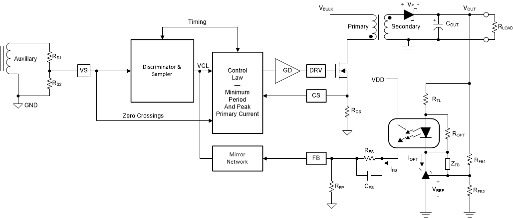
Figure 9 shows a simplified flyback convertor with the main output-regulation blocks of the device shown, along with typical implementation of secondary-side-derived regulation. The power-train operation is the same as any DCM-flyback circuit. A feedback current is optically coupled to the controller from a shunt-regulator sensing the output voltage.
 Figure 9. Simplified Flyback Converter
(with the Main Voltage Regulation Blocks)
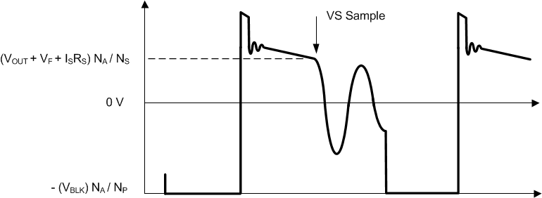
In this configuration, a secondary-side shunt-regulator, such as the TL431 (or ATL431), generates a current through the input photo-diode of an optocoupler. The photo-transistor delivers a proportional current that is dependent on the current-transfer ratio (CTR) of the optocoupler to the FB input of the UCC28742 controller. This FB current then converts into the VCL by the input-mirror network, detailed in the device block diagram (see Functional Block Diagram). Output-voltage variations convert to FB-current variations. The FB-current variations modify the VCL which dictates the appropriate IPP and fSW necessary to maintain CV regulation. At the same time, the VS input senses the auxiliary winding voltage during the transfer of transformer energy to the secondary output to monitor for an output overvoltage condition. When fSW reaches the converter target maximum frequency (i.e., corresponding de-mag time duty reaches 0.475), Constant Current Limit is triggered and further increases in VCL cannot increase fSW anymore. (see Figure 10, Control Law and Constant Current Limit and Delayed Shutdown)
 Figure 10. Auxiliary Winding Voltage
The UCC28742 samples the VS input voltage at the end of demagnetization time for output overvoltage detection and to determine the total demagnetization time for output current control in Constant Current Limit operation.
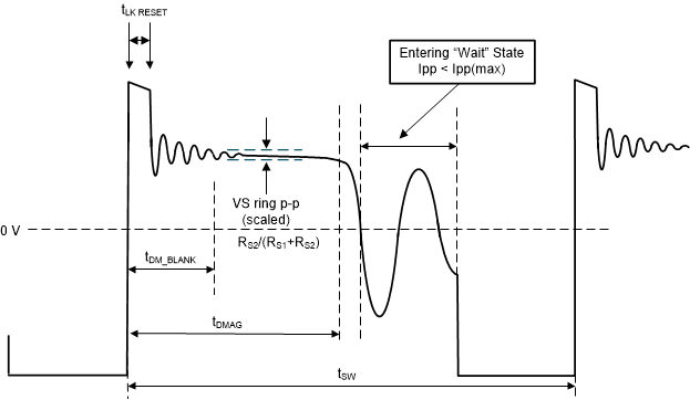
In order to maintain best performance of these functions the reset time and ringing of the auxiliary winding voltage should meet certain guidelines. Referring to Figure 11, the width of the leakage spike at the VS input should be less than tDM_BLANK. Minimum tDM_BLANK is 3 µs at maximum peak priamry current levels and proportionally less at lower peak primary current levels (the lowest 0.75 µs should be observed at high line and no load condition). In addition, any ringing following the spike should be reduced to < 160 mVpp (scaled to the VS pin) 200 ns before the end of the demagnetization time.
As mentioned in Device Functional Modes, when IPP< IPP(max), the device operation enters a “Wait” state during each switching cycle of its non-switching portion as shown in Figure 11. In the Wait state, the device bias current changes to IWAIT (typical 80 µA) from IRUN (typical 1.8 mA), reducing its bias power to help boost efficiency at light load and to reduce no-load input power.
 Figure 11. Auxiliary Waveform Details