SLUSER8C June 2022 – March 2023 UCC28C50 , UCC28C51 , UCC28C52 , UCC28C53 , UCC28C54 , UCC28C55 , UCC28C56H , UCC28C56L , UCC28C57H , UCC28C57L , UCC28C58 , UCC28C59 , UCC38C50 , UCC38C51 , UCC38C52 , UCC38C53 , UCC38C54 , UCC38C55
PRODUCTION DATA
- 1 Features
- 2 Applications
- 3 Description
- 4 Revision History
- 5 Device Comparison Table
- 6 Pin Configuration and Functions
- 7 Specifications
-
8 Detailed Description
- 8.1 Overview
- 8.2 Functional Block Diagram
- 8.3
Feature Description
- 8.3.1 Detailed Pin Description
- 8.3.2 Undervoltage Lockout
- 8.3.3 ±1% Internal Reference Voltage
- 8.3.4 Current Sense and Overcurrent Limit
- 8.3.5 Reduced-Discharge Current Variation
- 8.3.6 Oscillator Synchronization
- 8.3.7 Soft-Start Timing
- 8.3.8 Enable and Disable
- 8.3.9 Slope Compensation
- 8.3.10 Voltage Mode
- 8.4 Device Functional Modes
-
9 Application and Implementation
- 9.1 Application Information
- 9.2
Typical Application
- 9.2.1 Design Requirements
- 9.2.2
Detailed Design Procedure
- 9.2.2.1 Input Bulk Capacitor and Minimum Bulk Voltage
- 9.2.2.2 Transformer Turns Ratio and Maximum Duty Cycle
- 9.2.2.3 Transformer Inductance and Peak Currents
- 9.2.2.4 Output Capacitor
- 9.2.2.5 Current Sensing Network
- 9.2.2.6 Gate Drive Resistor
- 9.2.2.7 VREF Capacitor
- 9.2.2.8 RT/CT
- 9.2.2.9 Start-Up Circuit
- 9.2.2.10 Voltage Feedback Compensation
- 9.2.3 Application Curves
- 9.3 Power Supply Recommendations
- 9.4 Layout
- 10Device and Documentation Support
- 11Mechanical, Packaging, and Orderable Information
Package Options
Mechanical Data (Package|Pins)
- D|8
Thermal pad, mechanical data (Package|Pins)
Orderable Information
9.2 Typical Application
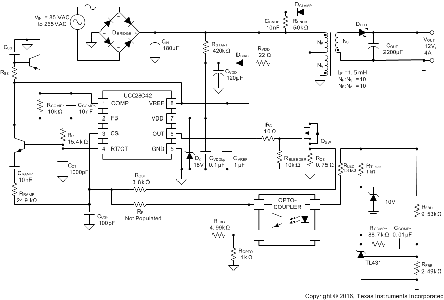
A typical application for the UCC28C42 controller in an off-line flyback converter is shown in Figure 9-3. The UCC28C52 controller can be used as drop-in replacement for UCC28C42.The controller uses an inner current control loop that contains a small current sense resistor which senses the primary inductor current ramp. This current sense resistor transforms the inductor current waveform to a voltage signal that is input directly into the primary side PWM comparator. This inner loop determines the response to input voltage changes. An outer voltage control loop involves comparing a portion of the output voltage to a reference voltage at the input of an error amplifier. When used in an off-line isolated application, the voltage feedback of the isolated output is accomplished using a secondary-side error amplifier and adjustable voltage reference, such as the TL431. The error signal crosses the primary to secondary isolation boundary using an opto-isolator whose collector is connected to the VREF pin and the emitter is connected to FB. The outer voltage control loop determines the response to load changes.
 Figure 9-3 Typical Application Design
Schematic