SLUS652E March 2005 – April 2020 UCD8220
PRODUCTION DATA.
- 1 Features
- 2 Applications
- 3 Description
- 4 Revision History
- 5 Pin Configuration and Functions
- 6 Specifications
- 7 Detailed Description
- 8 Application and Implementation
- 9 Power Supply Recommendations
- 10Layout
- 11Device and Documentation Support
- 12Mechanical, Packaging, and Orderable Information
Package Options
Refer to the PDF data sheet for device specific package drawings
Mechanical Data (Package|Pins)
- PWP|16
Thermal pad, mechanical data (Package|Pins)
- PWP|16
Orderable Information
8.2.2.3 Selecting the ISET Resistor for Peak Current Mode Control with Internal Slope Compensation
 Figure 34. UCD8220 Configured in Peak Current Control with Internal Slope Compensation
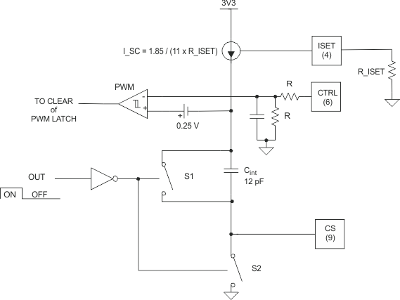
 When the ISET resistor is configured as shown in Figure 34 with the ISET resistor connected between the ISET pin and the AGND pin, the device is configured for peak current-mode control with internal slope compensation. The voltage at the ISET pin is 1.85 V so the internal slope compensation current, I_SC, being fed into the internal slope compensation capacitor is equal to 1.85 / (11 × R_ISET). Use Equation 7 to calculate the voltage slope at the PWM comparator input which is generated by this current.

 Figure 35. Slope vs R_ISET Resistance
 The amount of slope compensation required depends on the design of the power stage and the output specifications. A general rule is to add an up-slope equal to the down slope of the output inductor. Refer to (1) and (8) in the Related Documentation section for a more detailed discussion regarding slope compensation in peak current mode controlled power stages.