SBOS061C February 1997 – October 2024 XTR105
PRODUCTION DATA
- 1
- 1 Features
- 2 Applications
- 3 Description
- 4 Pin Configuration and Functions
- 5 Specifications
- 6 Detailed Description
- 7 Application and Implementation
- 8 Device and Documentation Support
- 9 Revision History
- 10Mechanical, Packaging, and Orderable Information
Package Options
Refer to the PDF data sheet for device specific package drawings
Mechanical Data (Package|Pins)
- D|14
- N|14
Thermal pad, mechanical data (Package|Pins)
Orderable Information
7.1.1 External Transistor
Transistor Q1 conducts the majority of the signal-dependent 4-20mA loop current. Using an external transistor isolates the majority of the power dissipation from the precision input and reference circuitry of the XTR105, maintaining excellent accuracy.
The external transistor is inside a feedback loop; therefore, the transistor characteristics are not critical. Requirements are: VCEO = 45V min, β = 40 min, and PD = 800mW. Power dissipation requirements can be lower if the loop power-supply voltage is less than 36V. Some possible choices for Q1 are listed in Figure 7-1.
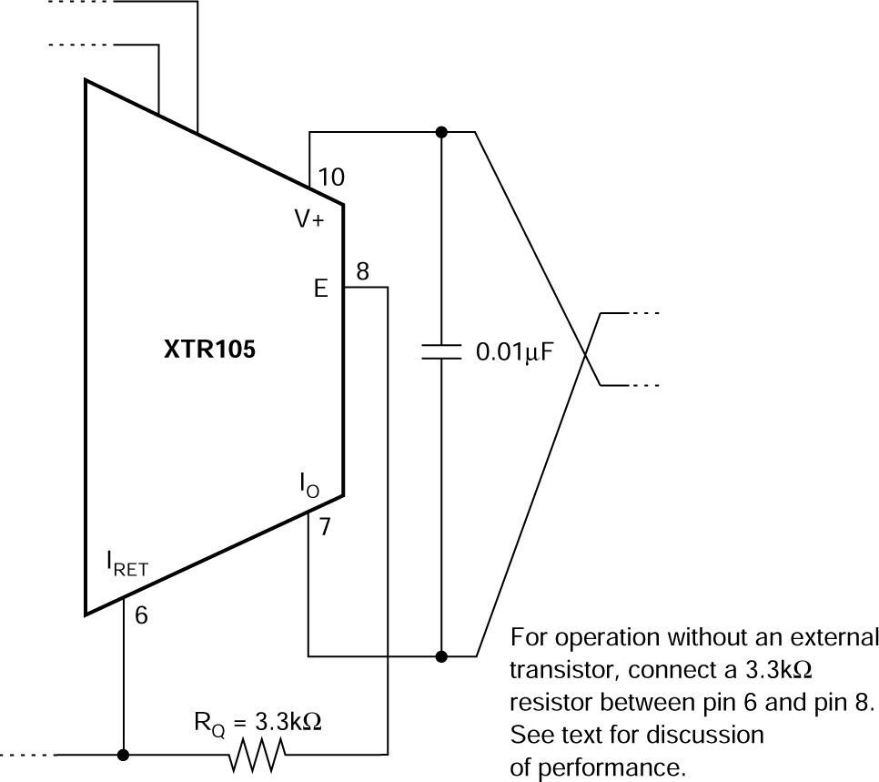
The XTR105 operates without this external transistor; however, accuracy is somewhat degraded as a result of the internal power dissipation and resulting self-heating. Operation without Q1 is not recommended for extended temperature ranges. A resistor (R = 3.3kΩ) connected between the IRET pin and the E (emitter) pin is advised for operation below 0°C without Q1 to support the full 20mA full-scale output, especially with V+ near 7.5V.
 Figure 7-2 Operation Without an External
Transistor