SBOS061C February 1997 – October 2024 XTR105
PRODUCTION DATA
- 1
- 1 Features
- 2 Applications
- 3 Description
- 4 Pin Configuration and Functions
- 5 Specifications
- 6 Detailed Description
- 7 Application and Implementation
- 8 Device and Documentation Support
- 9 Revision History
- 10Mechanical, Packaging, and Orderable Information
Package Options
Refer to the PDF data sheet for device specific package drawings
Mechanical Data (Package|Pins)
- D|14
- N|14
Thermal pad, mechanical data (Package|Pins)
Orderable Information
7.1 Application Information
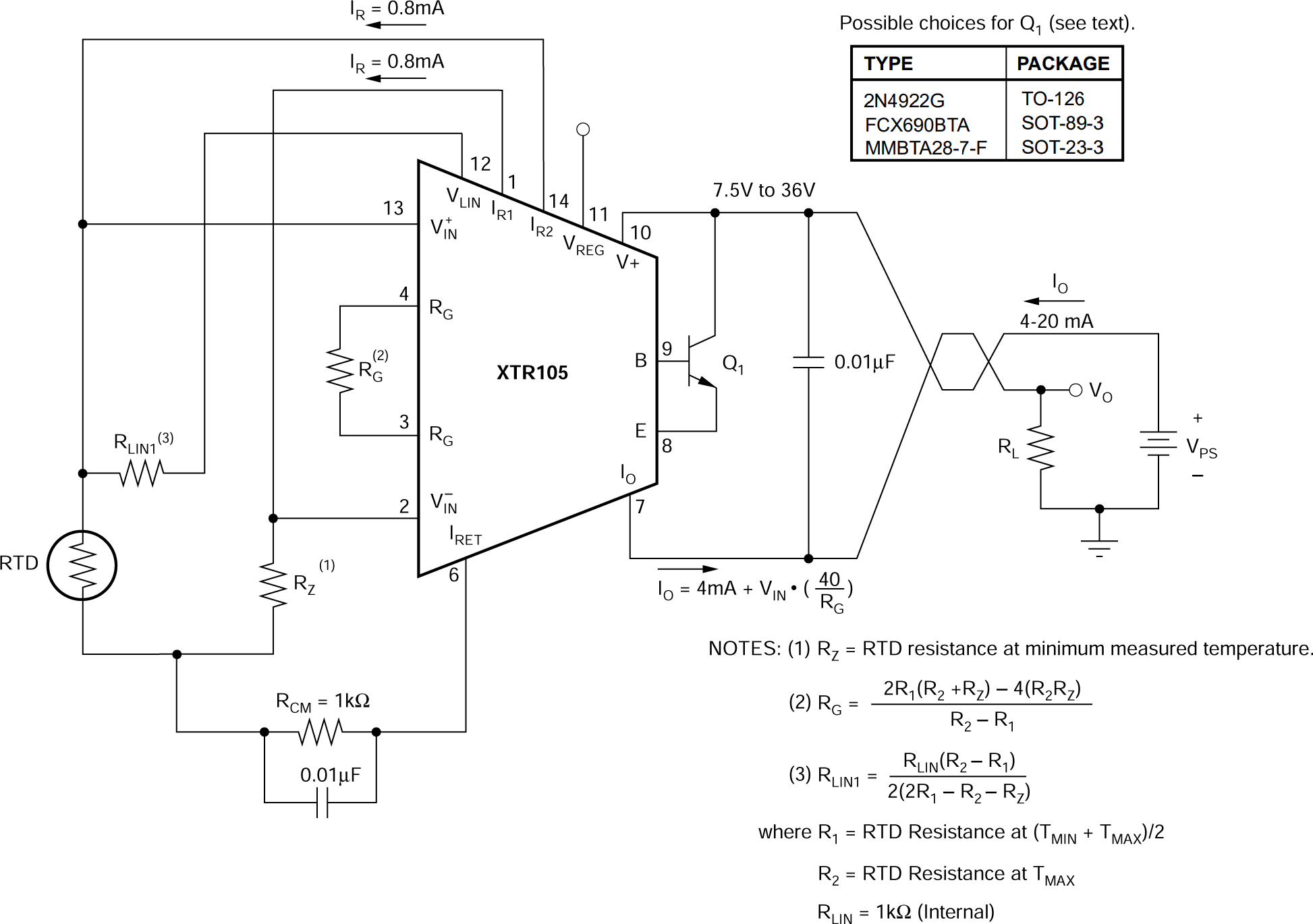
Figure 7-1 shows the basic connection diagram for the XTR105. The loop power supply, VPS, provides power for all circuitry. Output loop current is measured as a voltage across the series load resistor, RL.
Two matched 0.8mA current sources drive the RTD and zero-setting resistor, RZ. The instrumentation amplifier input of the XTR105 measures the voltage difference between the RTD and RZ. The value of RZ is chosen to be equal to the resistance of the RTD at the low-scale (minimum) measurement temperature. RZ can be adjusted to achieve 4mA output at the minimum measurement temperature to correct for input offset voltage and reference current mismatch of the XTR105.
RCM provides an additional voltage drop to bias the inputs of the XTR105 within the common-mode input range. Bypass RCM with a 0.01µF capacitor to minimize common-mode noise. Resistor RG sets the gain of the instrumentation amplifier according to the desired temperature range. RLIN1 provides 2nd-order linearization correction to the RTD, typically achieving a 40:1 improvement in linearity. An additional resistor is required for 3-wire RTD connections (see Figure 6-3).
The transfer function through the complete instrumentation amplifier and voltage-to-current converter is:
IO = 4mA + VIN × (40 / RG)
(VIN in volts, RG in ohms)
where VIN is the differential input voltage.
A negative input voltage, VIN, causes the output current to be less than 4mA. Increasingly negative VIN causes the output current to limit at approximately 2.2mA. See also typical characteristic Under-Scale Current vs Temperature.
Increasingly positive input voltage (greater than the full-scale input) produces increasing output current according to the transfer function, up to the output current limit of approximately 27mA. See also typical characteristic Over-Scale Current vs Temperature.
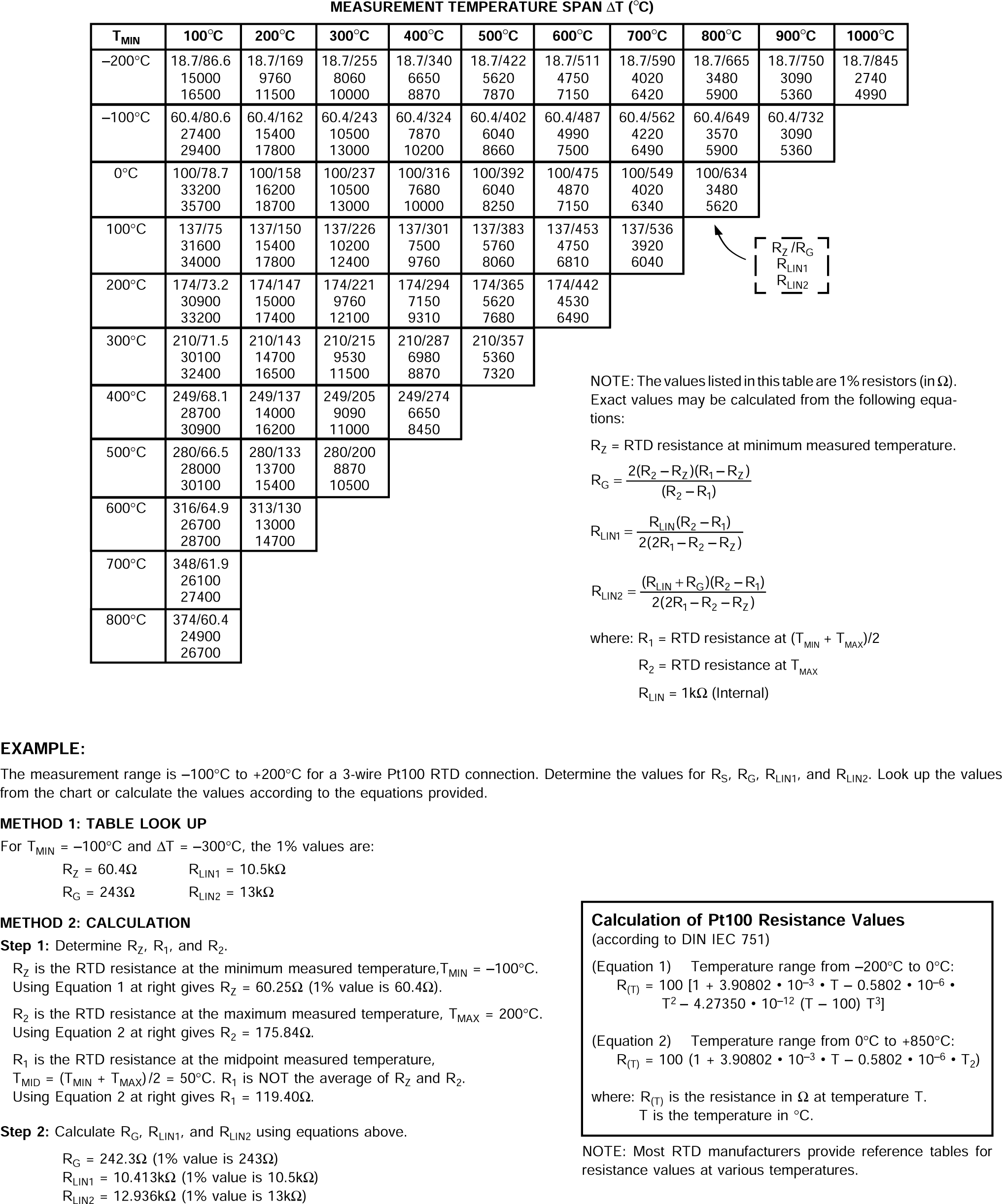
As evident from the transfer function, if no RG is used the gain is zero and the output is simply the XTR105’s zero current. The value of RG varies slightly for 2-wire RTD and 3-wire RTD connections with linearization. RG can be calculated from the equations given in Figure 7-1 (2-wire RTD connection) and Table 7-1 (3-wire RTD connection).
The IRET pin is the return path for all current from the current sources and VREG. The IRET pin allows any current used in external circuitry to be sensed by the XTR105 and to be included in the output current without causing an error.
 Figure 7-1 Basic 2-Wire RTD Temperature
Measurement Circuit With Linearization

|