SBOS913 February 2018 XTR305
PRODUCTION DATA.
- 1 Features
- 2 Applications
- 3 Description
- 4 Revision History
- 5 Pin Configuration and Functions
-
6 Specifications
- 6.1 Absolute Maximum Ratings
- 6.2 ESD Ratings
- 6.3 Recommended Operating Conditions
- 6.4 Thermal Information
- 6.5 Electrical Characteristics: Voltage Output Mode
- 6.6 Electrical Characteristics: Current Output Mode
- 6.7 Electrical Characteristics: Operational Amplifier (OPA)
- 6.8 Electrical Characteristics: Instrumentation Amplifier (IA)
- 6.9 Electrical Characteristics: Current Monitor
- 6.10 Electrical Characteristics: Power and Digital
- 6.11 Typical Characteristics
- 7 Detailed Description
-
8 Application and Implementation
- 8.1 Application Information
- 8.2
Typical Application
- 8.2.1 Design Requirements
- 8.2.2
Detailed Design Procedure
- 8.2.2.1 Voltage Output Mode
- 8.2.2.2 Current Output Mode
- 8.2.2.3 Input Signal Connection
- 8.2.2.4 Externally-Configured Mode: OPA and IA
- 8.2.2.5 Driver Output Disable
- 8.2.2.6 Driving Capacitive Loads and Loop Compensation
- 8.2.2.7 Internal Current Sources, Switching Noise, and Settling Time
- 8.2.2.8 IA Structure, Voltage Monitor
- 8.2.2.9 Digital I/O and Ground Considerations
- 8.2.2.10 Output Protection
- 8.2.3 Application Curves
- 9 Power Supply Recommendations
- 10Layout
- 11Device and Documentation Support
- 12Mechanical, Packaging, and Orderable Information
Package Options
Mechanical Data (Package|Pins)
- RGW|20
Thermal pad, mechanical data (Package|Pins)
- RGW|20
Orderable Information
8.2.2.10 Output Protection
The XTR305 is intended to operate in a harsh industrial environment. Therefore, a robust semiconductor process was chosen for this design. However, some external protection is still required.
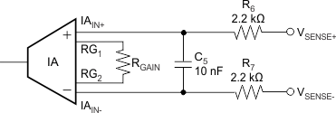
The instrumentation amplifier inputs can be protected by external resistors that limit current into the protection cell behind the IC pins, as shown in Figure 45. This cell conducts to the power-supply connection through a diode as soon as the input voltage exceeds the supply voltage. The circuit configuration example shows how to arrange these two external resistors.
The bias current is best cancelled if both resistors are equal. The additional capacitor reduces RF noise in the input signal to the IA.
 Figure 45. Current-Limiting Resistors
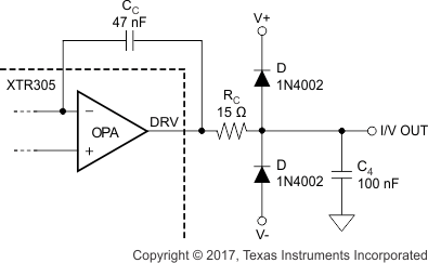
The load connection to the DRV output must be low impedance; therefore, external protection diodes may be necessary to handle excessive currents, as shown in Figure 46. The internal protection diodes start to conduct earlier than a normal external PN-type diode because they are affected by the higher die temperature. Therefore, either Schottky diodes are required, or an additional resistor (RC) can be placed in series with the input. An example of this protection is shown in Figure 46. Assuming the standard diodes limit the voltage to 1.4 V and the internal diodes clamp at 0.7 V, this resistor can limit the current into the internal protection diodes to 50 mA shown in Equation 7:

RC is also part of the recommended loop compensation. C4 helps protect the output against RFI and high-voltage spikes.
 Figure 46. Example for DRV Output Protection