-
CSD95378BQ5M Synchronous Buck NexFET Smart Power Stage
Package Options
Refer to the PDF data sheet for device specific package drawings
Mechanical Data (Package|Pins)
- DQP|12
Thermal pad, mechanical data (Package|Pins)
Orderable Information
CSD95378BQ5M Synchronous Buck NexFET Smart Power Stage
1 Features
- 60-A Continuous Operating Current Capability
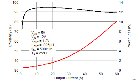
- 93.4% System Efficiency at 30 A
- Low-Power Loss of 2.8 W at 30 A
- High-Frequency Operation (up to 1.25 MHz)
- Diode Emulation Mode With FCCM
- Temperature Compensated Bi-Directional Current Sense
- Analog Temperature Output (400 mV at 0°C)
- Fault Monitoring
- High-Side Short, Overcurrent, and Overtemperature Protection
- 3.3-V and 5-V PWM Signal Compatible
- Tri-State PWM Input
- Integrated Bootstrap Diode
- Optimized Dead Time for Shoot-Through Protection
- High-Density SON 5-mm × 6-mm Footprint
- Ultra-Low-Inductance Package
- System Optimized PCB Footprint
- RoHS Compliant – Lead-Free Terminal Plating
- Halogen Free
2 Applications
- Multiphase Synchronous Buck Converters
- High-Frequency Applications
- High-Current, Low-Duty-Cycle Applications
- POL DC-DC Converters
- Memory and Graphic Cards
- Desktop and Server VR11.x / VR12.x V-core and Memory Synchronous Converters
3 Description
The CSD95378BQ5M NexFET™ smart power stage is a highly optimized design for use in a high-power, high-density synchronous buck converter. This product integrates the driver IC and power MOSFETs to complete the power stage switching function. This combination produces high-current, high-efficiency, and high speed switching capability in a small
5-mm × 6-mm outline package. It also integrates the accurate current sensing and temperature sensing functionality to simplify system design and improve accuracy. In addition, the PCB footprint is optimized to help reduce design time and simplify the completion of the overall system design.
Device Information(1)
| DEVICE | MEDIA | QTY | PACKAGE | SHIP |
|---|---|---|---|---|
| CSD95378BQ5M | 13-Inch Reel | 2500 | SON 5.00-mm × 6.00-mm Package |
Tape and Reel |
| CSD95378BQ5MT | 7-Inch Reel | 250 |
- For all available packages, see the orderable addendum at the end of the data sheet.
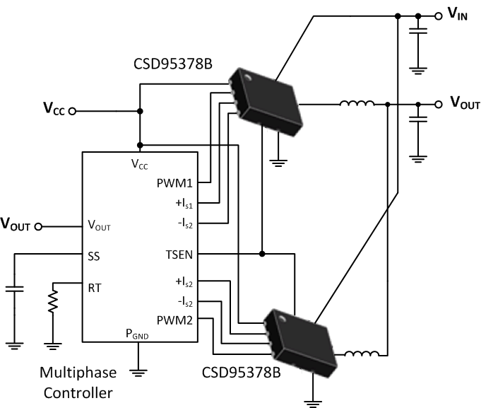
Application Diagram

Typical Power Stage Efficiency and Power Loss

4 Revision History
Changes from A Revision (July 2014) to B Revision
- Updated the CSD95378B parts in the Application SchematicGo
- Added the Receiving Notification of Documentation Updates and Community Resources sections in Device and Documentation SupportGo
Changes from * Revision (April 2014) to A Revision
- Updated the controller IC in the Application Schematic to the TPS40428Go
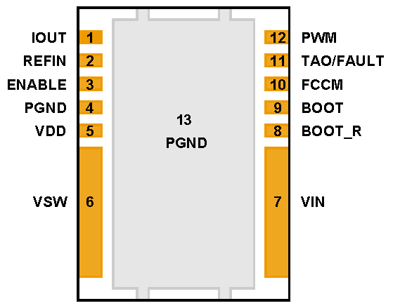
5 Pin Configuration and Functions

Pin Functions
| PIN | DESCRIPTION | |
|---|---|---|
| NAME | NO. | |
| BOOT | 9 | Bootstrap capacitor connection. Connect a minimum of 0.1-µF, 16-V, X7R ceramic capacitor from BOOT to BOOT_R pins. The bootstrap capacitor provides the charge to turn on the control FET. The bootstrap diode is integrated. |
| BOOT_R | 8 | Return path for HS gate driver, connected to VSW internally. |
| ENABLE | 3 | Enables device operation. If ENABLE = logic HIGH, turns on device. If ENABLE = logic LOW, the device is turned off and both MOSFET gates are actively pulled low. An internal 100-kΩ pulldown resistor will pull the ENABLE pin LOW if left floating. |
| FCCM | 10 | This pin enables the Diode Emulation function. When this pin is held LOW, Diode Emulation Mode is enabled for sync FET. When FCCM is HIGH, the device is operated in Forced Continuous Conduction Mode. An internal 5-µA current source will pull the FCCM pin to 3.3 V if left floating. |
| IOUT | 1 | Output of current sensing amplifier. V(IOUT) – V(REFIN) is proportional to the phase current. |
| PGND | 4 | Power ground, connected directly to pin 13. |
| PGND | 13 | Power ground. |
| PWM | 12 | Pulse width modulated tri-state input from external controller. Logic LOW sets control FET gate low and sync FET gate high. Logic HIGH sets control FET gate high and sync FET gate low. Open or Hi-Z sets both MOSFET gates low if greater than the tri-state shutdown hold-off time (t3HT). |
| REFIN | 2 | External reference voltage input for current sensing amplifier. |
| TAO/ FAULT |
11 | Temperature analog output. Reports a voltage proportional to the die temperature. An ORing diode is integrated in the IC. When used in multiphase application, a single wire can be used to connect the TAO pins of all the ICs. Only the highest temperature will be reported. TAO will be pulled up to 3.3 V if thermal shutdown occurs. TAO should be bypassed to PGND with a 1-nF, 16-V, X7R ceramic capacitor. |
| VDD | 5 | Supply voltage to gate driver and internal circuitry. |
| VIN | 7 | Input voltage pin. Connect input capacitors close to this pin. |
| VSW | 6 | Phase node connecting the HS MOSFET source and LS MOSFET drain - pin connection to the output inductor. |