JAJSFW1E June 2017 – March 2019 66AK2G12
PRODUCTION DATA.
- 1デバイスの概要
- 2改訂履歴
- 3Device Comparison
-
4Terminal Configuration and Functions
- 4.1 Pin Diagram
- 4.2 Pin Attributes
- 4.3 Signal Descriptions
- 4.4 Pin Multiplexing
- 4.5 Connections for Unused Pins
-
5Specifications
- 5.1 Absolute Maximum Ratings
- 5.2 ESD Ratings
- 5.3 Power-On-Hour (POH) Limits
- 5.4 Recommended Operating Conditions
- 5.5 Operating Performance Points
- 5.6 Power Consumption Summary
- 5.7
Electrical Characteristics
- Table 5-2 DDR3L SSTL DC Electrical Characteristics
- Table 5-3 I2C OPEN DRAIN DC Electrical Characteristics
- Table 5-4 Oscillators DC Electrical Characteristics
- Table 5-5 LVDS Input Buffer DC Electrical Characteristics
- Table 5-6 LVDS Output Buffer DC Electrical Characteristics
- Table 5-7 MLB LVDS Buffers DC Electrical Characteristics
- Table 5-8 PORn DC Electrical Characteristics
- Table 5-9 1.8-Volt I/O LVCMOS DC Electrical Characteristics
- Table 5-10 3.3-Volt I/O LVCMOS DC Electrical Characteristics
- 5.7.1 USB0_PHY and USB1_PHY DC Electrical Characteristics
- 5.7.2 PCIe SERDES DC Electrical Characteristics
- 5.8 Thermal Resistance Characteristics for ABY Package
- 5.9
Timing and Switching Characteristics
- 5.9.1 Power Supply Sequencing
- 5.9.2 Reset Timing
- 5.9.3
Clock Specifications
- 5.9.3.1 Input Clocks / Oscillators
- 5.9.3.2 Optional LVDS Clock Inputs Not Used
- 5.9.3.3 Optional Audio Oscillator (AUDOSC) with External Crystal Circuit
- 5.9.3.4 Optional Audio Oscillator (AUDOSC) with External LVCMOS Clock Source
- 5.9.3.5 Optional Audio Oscillator (AUDOSC) Not Used
- 5.9.3.6 Optional USB PHY Reference Clock
- 5.9.3.7 PCIe Reference Clock
- 5.9.3.8 Output Clocks
- 5.9.3.9 PLLs
- 5.9.3.10 Recommended Clock and Control Signal Transition Behavior
- 5.9.4
Peripherals
- 5.9.4.1 DCAN
- 5.9.4.2 DSS
- 5.9.4.3 DDR EMIF
- 5.9.4.4
EMAC
- 5.9.4.4.1 EMAC MDIO Interface Timings
- 5.9.4.4.2
EMAC MII Timings
- Table 5-28 Timing Requirements for MII_RXCLK—MII Operation
- Table 5-29 Timing Requirements for MII_TXCLK—MII Operation
- Table 5-30 Timing Requirements for EMAC MII Receive 10 Mbps and 100 Mbps
- Table 5-31 Switching Characteristics Over Recommended Operating Conditions for EMAC MII Transmit 10 Mbps and 100 Mbps
- 5.9.4.4.3
EMAC RMII Timings
- Table 5-32 Timing Requirements for EMAC RMII_REFCLK—RMII Operation
- Table 5-33 Timing Requirements for EMAC RMII Receive
- Table 5-34 Switching Characteristics Over Recommended Operating Conditions for EMAC RMII_REFCLK —RMII Operation
- Table 5-35 Switching Characteristics Over Recommended Operating Conditions for EMAC RMII Transmit 10 Mbps and 100 Mbps
- 5.9.4.4.4
EMAC RGMII Timings
- Table 5-36 Timing Requirements for RGMII_RXC—RGMII Operation
- Table 5-37 Timing Requirements for EMAC RGMII Input Receive for 10 Mbps, 100 Mbps, and 1000 Mbps
- Table 5-38 Switching Characteristics Over Recommended Operating Conditions for Transmit - RGMII operation for 10 Mbps, 100 Mbps, and 1000 Mbps
- Table 5-39 Switching Characteristics Over Recommended Operating Conditions for EMAC RGMII Transmit - RGMII_TXD[3:0], and RGMII_TXCTL - RGMII Mode
- Table 5-40 Switching Characteristics Over Recommended Operating Conditions for EMAC RGMII Transmit - RGMII_TXD[3:0], and RGMII_TXCTL - RGMII ID Mode
- 5.9.4.5 GPMC
- 5.9.4.6 I2C
- 5.9.4.7 McASP
- 5.9.4.8 McBSP
- 5.9.4.9 MLB
- 5.9.4.10
MMC/SD
- Table 5-60 MMC Timing Conditions
- Table 5-61 Timing Requirements for MMC0_CMD and MMC0_DATn
- Table 5-62 Timing Requirements for MMC1_CMD and MMC1_DATn when operating in SDR mode
- Table 5-63 Timing Requirements for MMC1_CMD and MMC1_DATn when operating in DDR mode
- Table 5-64 Switching Characteristics for MMCi_CLK
- Table 5-65 Switching Characteristics for MMC0_CMD and MMC0_DATn—HSPE=0
- Table 5-66 Switching Characteristics for MMC1_CMD and MMC1_DATn—HSPE=0 when operating in SDR mode
- Table 5-67 Switching Characteristics for MMC1_CMD and MMC1_DATn—HSPE=0 when operating in DDR mode
- 5.9.4.11 PCIESS
- 5.9.4.12
PRU-ICSS
- 5.9.4.12.1 Programmable Real-Time Unit (PRU-ICSS PRU)
- 5.9.4.12.2 PRU-ICSS EtherCAT (PRU-ICSS ECAT)
- 5.9.4.12.3 PRU-ICSS MII_RT and Switch
- 5.9.4.12.4 PRU-ICSS Universal Asynchronous Receiver Transmitter (PRU-ICSS UART)
- 5.9.4.12.5 PRU-ICSS PRU Sigma Delta and EnDAT Modes
- 5.9.4.13 QSPI
- 5.9.4.14 SPI
- 5.9.4.15 Timers
- 5.9.4.16 UART
- 5.9.4.17 USB
- 5.9.5 Emulation and Debug Subsystem
- 6Detailed Description
-
7Applications, Implementation, and Layout
- 7.1
DDR3L Board Design and Layout Guidelines
- 7.1.1 DDR3L General Board Layout Guidelines
- 7.1.2
DDR3L Board Design and Layout Guidelines
- 7.1.2.1 Board Designs
- 7.1.2.2 DDR3L Device Combinations
- 7.1.2.3 DDR3L Interface Schematic
- 7.1.2.4 Compatible JEDEC DDR3L Devices
- 7.1.2.5 PCB Stackup
- 7.1.2.6 Placement
- 7.1.2.7 DDR3L Keepout Region
- 7.1.2.8 Bulk Bypass Capacitors
- 7.1.2.9 High-Speed Bypass Capacitors
- 7.1.2.10 Net Classes
- 7.1.2.11 DDR3L Signal Termination
- 7.1.2.12 VREF_DDR Routing
- 7.1.2.13 VTT
- 7.1.2.14 CK and ADDR_CTRL Topologies and Routing Definition
- 7.1.2.15 Data Topologies and Routing Definition
- 7.1.2.16 Routing Specification
- 7.2 High Speed Differential Signal Routing Guidance
- 7.3 Power Distribution Network (PDN) Implementation Guidance
- 7.4 Single-Ended Interfaces
- 7.5 Clock Routing Guidelines
- 7.1
DDR3L Board Design and Layout Guidelines
- 8Device and Documentation Support
- 9Mechanical Packaging and Orderable Information
パッケージ・オプション
デバイスごとのパッケージ図は、PDF版データシートをご参照ください。
メカニカル・データ(パッケージ|ピン)
- ABY|625
サーマルパッド・メカニカル・データ
発注情報
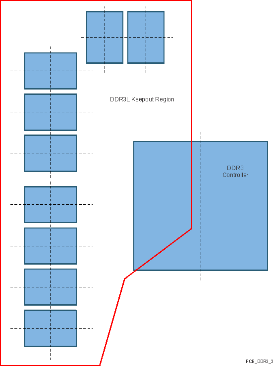
7.1.2.7 DDR3L Keepout Region
The region of the PCB used for DDR3L circuitry must be isolated from other signals. The DDR3L keepout region is defined for this purpose and is shown in Figure 7-5. The size of this region varies with the placement and DDR3L routing. Additional clearances required for the keepout region are shown in Table 7-6. Non-DDR3L signals should not be routed on the DDR3L signal layers within the DDR3L keepout region. Non-DDR3L signals may be routed in the region, provided they are routed on layers separated from the DDR3L signal layers by a ground layer. No breaks should be allowed in the reference ground layers in this region. In addition, the DVDD_DDR power plane should cover the entire keepout region. Also note that the two signals from the DDR3L controller should be separated from each other by the specification in Table 7-6 (see KOD37).
 Figure 7-5 DDR3L Keepout Region