JAJSFW1E June 2017 – March 2019 66AK2G12
PRODUCTION DATA.
- 1デバイスの概要
- 2改訂履歴
- 3Device Comparison
-
4Terminal Configuration and Functions
- 4.1 Pin Diagram
- 4.2 Pin Attributes
- 4.3 Signal Descriptions
- 4.4 Pin Multiplexing
- 4.5 Connections for Unused Pins
-
5Specifications
- 5.1 Absolute Maximum Ratings
- 5.2 ESD Ratings
- 5.3 Power-On-Hour (POH) Limits
- 5.4 Recommended Operating Conditions
- 5.5 Operating Performance Points
- 5.6 Power Consumption Summary
- 5.7
Electrical Characteristics
- Table 5-2 DDR3L SSTL DC Electrical Characteristics
- Table 5-3 I2C OPEN DRAIN DC Electrical Characteristics
- Table 5-4 Oscillators DC Electrical Characteristics
- Table 5-5 LVDS Input Buffer DC Electrical Characteristics
- Table 5-6 LVDS Output Buffer DC Electrical Characteristics
- Table 5-7 MLB LVDS Buffers DC Electrical Characteristics
- Table 5-8 PORn DC Electrical Characteristics
- Table 5-9 1.8-Volt I/O LVCMOS DC Electrical Characteristics
- Table 5-10 3.3-Volt I/O LVCMOS DC Electrical Characteristics
- 5.7.1 USB0_PHY and USB1_PHY DC Electrical Characteristics
- 5.7.2 PCIe SERDES DC Electrical Characteristics
- 5.8 Thermal Resistance Characteristics for ABY Package
- 5.9
Timing and Switching Characteristics
- 5.9.1 Power Supply Sequencing
- 5.9.2 Reset Timing
- 5.9.3
Clock Specifications
- 5.9.3.1 Input Clocks / Oscillators
- 5.9.3.2 Optional LVDS Clock Inputs Not Used
- 5.9.3.3 Optional Audio Oscillator (AUDOSC) with External Crystal Circuit
- 5.9.3.4 Optional Audio Oscillator (AUDOSC) with External LVCMOS Clock Source
- 5.9.3.5 Optional Audio Oscillator (AUDOSC) Not Used
- 5.9.3.6 Optional USB PHY Reference Clock
- 5.9.3.7 PCIe Reference Clock
- 5.9.3.8 Output Clocks
- 5.9.3.9 PLLs
- 5.9.3.10 Recommended Clock and Control Signal Transition Behavior
- 5.9.4
Peripherals
- 5.9.4.1 DCAN
- 5.9.4.2 DSS
- 5.9.4.3 DDR EMIF
- 5.9.4.4
EMAC
- 5.9.4.4.1 EMAC MDIO Interface Timings
- 5.9.4.4.2
EMAC MII Timings
- Table 5-28 Timing Requirements for MII_RXCLK—MII Operation
- Table 5-29 Timing Requirements for MII_TXCLK—MII Operation
- Table 5-30 Timing Requirements for EMAC MII Receive 10 Mbps and 100 Mbps
- Table 5-31 Switching Characteristics Over Recommended Operating Conditions for EMAC MII Transmit 10 Mbps and 100 Mbps
- 5.9.4.4.3
EMAC RMII Timings
- Table 5-32 Timing Requirements for EMAC RMII_REFCLK—RMII Operation
- Table 5-33 Timing Requirements for EMAC RMII Receive
- Table 5-34 Switching Characteristics Over Recommended Operating Conditions for EMAC RMII_REFCLK —RMII Operation
- Table 5-35 Switching Characteristics Over Recommended Operating Conditions for EMAC RMII Transmit 10 Mbps and 100 Mbps
- 5.9.4.4.4
EMAC RGMII Timings
- Table 5-36 Timing Requirements for RGMII_RXC—RGMII Operation
- Table 5-37 Timing Requirements for EMAC RGMII Input Receive for 10 Mbps, 100 Mbps, and 1000 Mbps
- Table 5-38 Switching Characteristics Over Recommended Operating Conditions for Transmit - RGMII operation for 10 Mbps, 100 Mbps, and 1000 Mbps
- Table 5-39 Switching Characteristics Over Recommended Operating Conditions for EMAC RGMII Transmit - RGMII_TXD[3:0], and RGMII_TXCTL - RGMII Mode
- Table 5-40 Switching Characteristics Over Recommended Operating Conditions for EMAC RGMII Transmit - RGMII_TXD[3:0], and RGMII_TXCTL - RGMII ID Mode
- 5.9.4.5 GPMC
- 5.9.4.6 I2C
- 5.9.4.7 McASP
- 5.9.4.8 McBSP
- 5.9.4.9 MLB
- 5.9.4.10
MMC/SD
- Table 5-60 MMC Timing Conditions
- Table 5-61 Timing Requirements for MMC0_CMD and MMC0_DATn
- Table 5-62 Timing Requirements for MMC1_CMD and MMC1_DATn when operating in SDR mode
- Table 5-63 Timing Requirements for MMC1_CMD and MMC1_DATn when operating in DDR mode
- Table 5-64 Switching Characteristics for MMCi_CLK
- Table 5-65 Switching Characteristics for MMC0_CMD and MMC0_DATn—HSPE=0
- Table 5-66 Switching Characteristics for MMC1_CMD and MMC1_DATn—HSPE=0 when operating in SDR mode
- Table 5-67 Switching Characteristics for MMC1_CMD and MMC1_DATn—HSPE=0 when operating in DDR mode
- 5.9.4.11 PCIESS
- 5.9.4.12
PRU-ICSS
- 5.9.4.12.1 Programmable Real-Time Unit (PRU-ICSS PRU)
- 5.9.4.12.2 PRU-ICSS EtherCAT (PRU-ICSS ECAT)
- 5.9.4.12.3 PRU-ICSS MII_RT and Switch
- 5.9.4.12.4 PRU-ICSS Universal Asynchronous Receiver Transmitter (PRU-ICSS UART)
- 5.9.4.12.5 PRU-ICSS PRU Sigma Delta and EnDAT Modes
- 5.9.4.13 QSPI
- 5.9.4.14 SPI
- 5.9.4.15 Timers
- 5.9.4.16 UART
- 5.9.4.17 USB
- 5.9.5 Emulation and Debug Subsystem
- 6Detailed Description
-
7Applications, Implementation, and Layout
- 7.1
DDR3L Board Design and Layout Guidelines
- 7.1.1 DDR3L General Board Layout Guidelines
- 7.1.2
DDR3L Board Design and Layout Guidelines
- 7.1.2.1 Board Designs
- 7.1.2.2 DDR3L Device Combinations
- 7.1.2.3 DDR3L Interface Schematic
- 7.1.2.4 Compatible JEDEC DDR3L Devices
- 7.1.2.5 PCB Stackup
- 7.1.2.6 Placement
- 7.1.2.7 DDR3L Keepout Region
- 7.1.2.8 Bulk Bypass Capacitors
- 7.1.2.9 High-Speed Bypass Capacitors
- 7.1.2.10 Net Classes
- 7.1.2.11 DDR3L Signal Termination
- 7.1.2.12 VREF_DDR Routing
- 7.1.2.13 VTT
- 7.1.2.14 CK and ADDR_CTRL Topologies and Routing Definition
- 7.1.2.15 Data Topologies and Routing Definition
- 7.1.2.16 Routing Specification
- 7.2 High Speed Differential Signal Routing Guidance
- 7.3 Power Distribution Network (PDN) Implementation Guidance
- 7.4 Single-Ended Interfaces
- 7.5 Clock Routing Guidelines
- 7.1
DDR3L Board Design and Layout Guidelines
- 8Device and Documentation Support
- 9Mechanical Packaging and Orderable Information
パッケージ・オプション
デバイスごとのパッケージ図は、PDF版データシートをご参照ください。
メカニカル・データ(パッケージ|ピン)
- ABY|625
サーマルパッド・メカニカル・データ
発注情報
7.1.2.14.1.2 CK and ADDR_CTRL Routing, Four DDR3L Devices
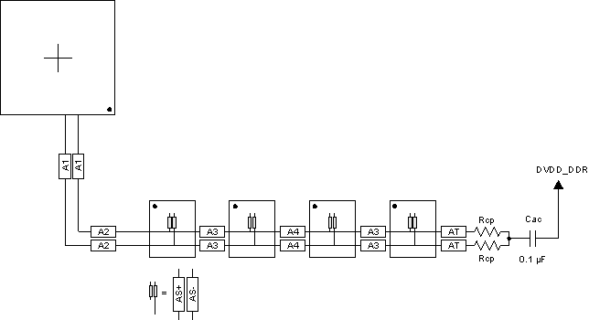
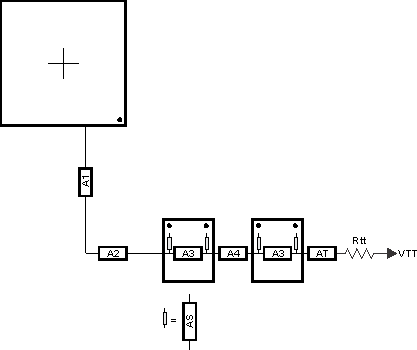
Figure 7-8 shows the CK routing for four DDR3L devices placed on the same side of the PCB. Figure 7-9 shows the corresponding ADDR_CTRL routing.
 Figure 7-8 CK Routing for Four Single-Side DDR3L Devices
  Figure 7-9 ADDR_CTRL Routing for Four Single-Side DDR3L Devices
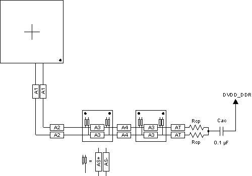
 To save PCB space, the four DDR3L memories may be mounted as two mirrored pairs at a cost of increased routing and assembly complexity. Figure 7-10 and Figure 7-11 show the routing for CK and ADDR_CTRL, respectively, for four DDR3L devices mirrored in a two-pair configuration.
 Figure 7-10 CK Routing for Four Mirrored DDR3L Devices
  Figure 7-11 ADDR_CTRL Routing for Four Mirrored DDR3L Devices