JAJSDJ8A April 2017 – October 2021 ADC12D1620QML-SP
PRODUCTION DATA
- 1 特長
- 2 アプリケーション
- 3 概要
- 4 Revision History
- 5 Pin Configuration and Functions
-
6 Specifications
- 6.1 Absolute Maximum Ratings
- 6.2 ESD Ratings
- 6.3 Recommended Operating Conditions
- 6.4 Thermal Information
- 6.5 Converter Electrical Characteristics: Static Converter Characteristics
- 6.6 Converter Electrical Characteristics: Dynamic Converter Characteristics
- 6.7 Converter Electrical Characteristics: Analog Input/Output and Reference Characteristics
- 6.8 Converter Electrical Characteristic: Channel-to-Channel Characteristics
- 6.9 Converter Electrical Characteristics: LVDS CLK Input Characteristics
- 6.10 Electrical Characteristics: AutoSync Feature
- 6.11 Converter Electrical Characteristics: Digital Control and Output Pin Characteristics
- 6.12 Converter Electrical Characteristics: Power Supply Characteristics
- 6.13 Converter Electrical Characteristics: AC Electrical Characteristics
- 6.14 Electrical Characteristics: Delta Parameters
- 6.15 Timing Requirements: Serial Port Interface
- 6.16 Timing Requirements: Calibration
- 6.17 Quality Conformance Inspection
- 6.18 Timing Diagrams
- 6.19 Typical Characteristics
-
7 Detailed Description
- 7.1 Overview
- 7.2 Functional Block Diagram
- 7.3 Feature Description
- 7.4 Device Functional Modes
- 7.5
Programming
- 7.5.1
Control Modes
- 7.5.1.1
Non-ECM
- 7.5.1.1.1 Dual-Edge Sampling Pin (DES)
- 7.5.1.1.2 Non-Demultiplexed Mode Pin (NDM)
- 7.5.1.1.3 Dual Data-Rate Phase Pin (DDRPh)
- 7.5.1.1.4 Calibration Pin (CAL)
- 7.5.1.1.5 Low-Sampling Power-Saving Mode Pin (LSPSM)
- 7.5.1.1.6 Power-Down I-Channel Pin (PDI)
- 7.5.1.1.7 Power-Down Q-Channel Pin (PDQ)
- 7.5.1.1.8 Test-Pattern Mode Pin (TPM)
- 7.5.1.1.9 Full-Scale Input-Range Pin (FSR)
- 7.5.1.1.10 AC- or DC-Coupled Mode Pin (VCMO)
- 7.5.1.1.11 LVDS Output Common-Mode Pin (VBG)
- 7.5.1.2 Extended Control Mode
- 7.5.1.1
Non-ECM
- 7.5.1
Control Modes
- 7.6 Register Maps
- 8 Application Information Disclaimer
- 9 Power Supply Recommendations
- 10Layout
- 11Device and Documentation Support
- 12Mechanical, Packaging, and Orderable Information
パッケージ・オプション
デバイスごとのパッケージ図は、PDF版データシートをご参照ください。
メカニカル・データ(パッケージ|ピン)
- FVA|256
- NAA|376
サーマルパッド・メカニカル・データ
発注情報
7.3.2.1 SDR / DDR Clock
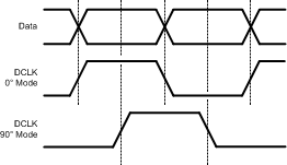
The ADC12D1620 output data can be delivered in double data rate (DDR) or single data rate (SDR). For DDR, the DCLK frequency is half the data rate, and data is sent to the outputs on both edges of DCLK; see Figure 7-1. The DCLK-to-data phase relationship may be either 0° or 90°. For 0° mode, the data transitions on each edge of the DCLK. Any offset from this timing is tOSK; (see Converter Electrical Characteristics: AC Electrical Characteristics for details). For 90° mode, the DCLK transitions in the middle of each data cell. Setup and hold times for this transition, tSU and tH, may also be found in Converter Electrical Characteristics: AC Electrical Characteristics. The DCLK-to-data phase relationship may be selected through the DDRPh pin in non-ECM (see Dual Data-Rate Phase Pin (DDRPh)) or the DPS bit in the Configuration Register (Addr: 0h; Bit: 14) in ECM. Note that for DDR mode, the 1:2 demux mode is not available in LSPSM.
 Figure 7-1 DDR DCLK-to-Data Phase Relationship
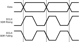
For SDR, the DCLK frequency is the same as the data rate, and data is sent to the outputs on a single edge of DCLK; see Figure 7-2. The data may transition on either the rising or falling edge of DCLK. Any offset from this timing is tOSK; see Converter Electrical Characteristics: AC Electrical Characteristics for details. The DCLK rising or falling edge may be selected through the SDR bit in the Configuration Register (Addr: 0h; Bit: 2) in ECM only.
 Figure 7-2 SDR DCLK-to-Data Phase Relationship