JAJSDJ8A April 2017 – October 2021 ADC12D1620QML-SP
PRODUCTION DATA
- 1 特長
- 2 アプリケーション
- 3 概要
- 4 Revision History
- 5 Pin Configuration and Functions
-
6 Specifications
- 6.1 Absolute Maximum Ratings
- 6.2 ESD Ratings
- 6.3 Recommended Operating Conditions
- 6.4 Thermal Information
- 6.5 Converter Electrical Characteristics: Static Converter Characteristics
- 6.6 Converter Electrical Characteristics: Dynamic Converter Characteristics
- 6.7 Converter Electrical Characteristics: Analog Input/Output and Reference Characteristics
- 6.8 Converter Electrical Characteristic: Channel-to-Channel Characteristics
- 6.9 Converter Electrical Characteristics: LVDS CLK Input Characteristics
- 6.10 Electrical Characteristics: AutoSync Feature
- 6.11 Converter Electrical Characteristics: Digital Control and Output Pin Characteristics
- 6.12 Converter Electrical Characteristics: Power Supply Characteristics
- 6.13 Converter Electrical Characteristics: AC Electrical Characteristics
- 6.14 Electrical Characteristics: Delta Parameters
- 6.15 Timing Requirements: Serial Port Interface
- 6.16 Timing Requirements: Calibration
- 6.17 Quality Conformance Inspection
- 6.18 Timing Diagrams
- 6.19 Typical Characteristics
-
7 Detailed Description
- 7.1 Overview
- 7.2 Functional Block Diagram
- 7.3 Feature Description
- 7.4 Device Functional Modes
- 7.5
Programming
- 7.5.1
Control Modes
- 7.5.1.1
Non-ECM
- 7.5.1.1.1 Dual-Edge Sampling Pin (DES)
- 7.5.1.1.2 Non-Demultiplexed Mode Pin (NDM)
- 7.5.1.1.3 Dual Data-Rate Phase Pin (DDRPh)
- 7.5.1.1.4 Calibration Pin (CAL)
- 7.5.1.1.5 Low-Sampling Power-Saving Mode Pin (LSPSM)
- 7.5.1.1.6 Power-Down I-Channel Pin (PDI)
- 7.5.1.1.7 Power-Down Q-Channel Pin (PDQ)
- 7.5.1.1.8 Test-Pattern Mode Pin (TPM)
- 7.5.1.1.9 Full-Scale Input-Range Pin (FSR)
- 7.5.1.1.10 AC- or DC-Coupled Mode Pin (VCMO)
- 7.5.1.1.11 LVDS Output Common-Mode Pin (VBG)
- 7.5.1.2 Extended Control Mode
- 7.5.1.1
Non-ECM
- 7.5.1
Control Modes
- 7.6 Register Maps
- 8 Application Information Disclaimer
- 9 Power Supply Recommendations
- 10Layout
- 11Device and Documentation Support
- 12Mechanical, Packaging, and Orderable Information
パッケージ・オプション
デバイスごとのパッケージ図は、PDF版データシートをご参照ください。
メカニカル・データ(パッケージ|ピン)
- FVA|256
- NAA|376
サーマルパッド・メカニカル・データ
発注情報
6.19 Typical Characteristics
VA = VDR = VTC = VE = 1.9 V, fCLK = 1600 MHz in non-LSPSM and 800 MHz in LSPSM, fIN = 248 MHz, TA= 25°C, 1:2 demux non-DES mode, and calibration performed after temperature, supply voltage or sample rate change, unless otherwise stated.
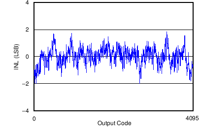 Figure 6-11 INL vs Code
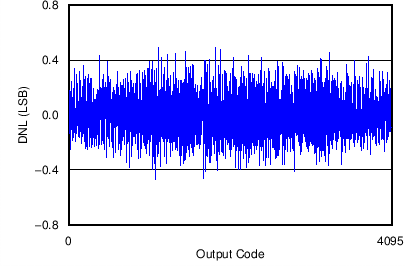 Figure 6-13 DNL vs Code
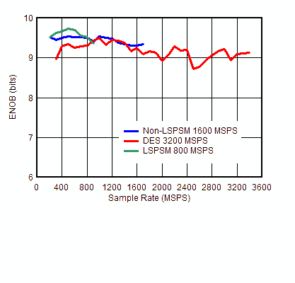 Figure 6-15 ENOB vs Sample Rate
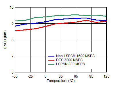 Figure 6-17 ENOB vs Temperature
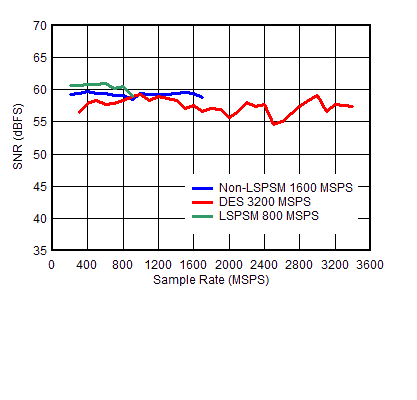 Figure 6-19 SNR vs Sample Rate
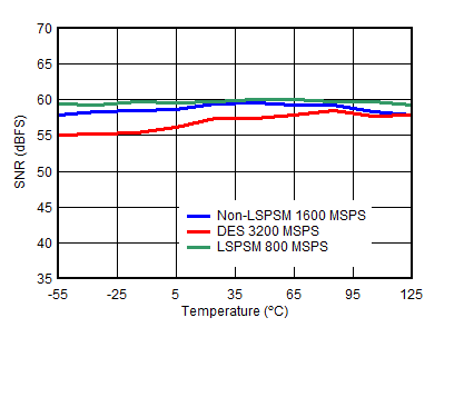 Figure 6-21 SNR vs Temperature
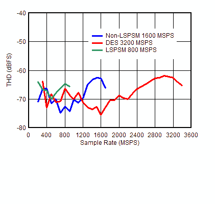 Figure 6-23 THD vs Sample Rate
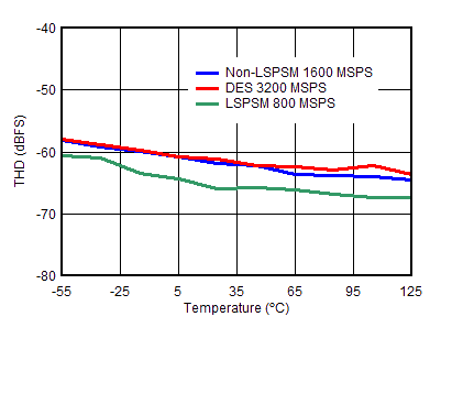 Figure 6-25 THD vs Temperature
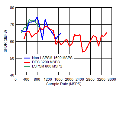 Figure 6-27 SFDR vs Sample Rate
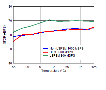 Figure 6-29 SFDR vs Temperature
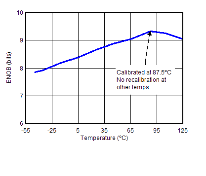
| fCLK = 1.6 GHz | fIN = 248 MHz |
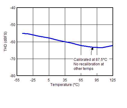
| fCLK = 1.6 GHz | fIN = 248 MHz |
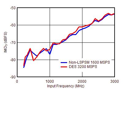 Figure 6-35 3rd Order Intermodulation Distortion vs Input Frequency
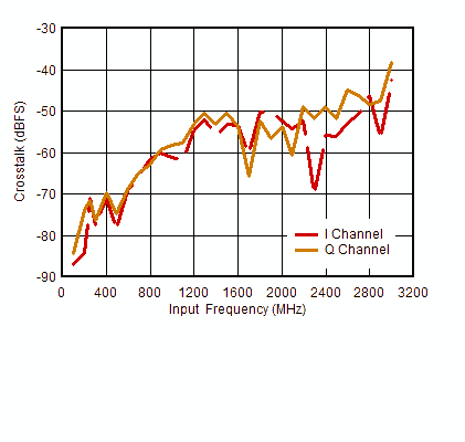 Figure 6-37 Cross Talk vs Input Frequency
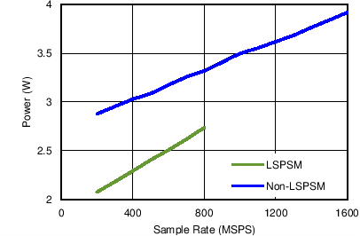 Figure 6-39 Power Consumption vs Sample Rate
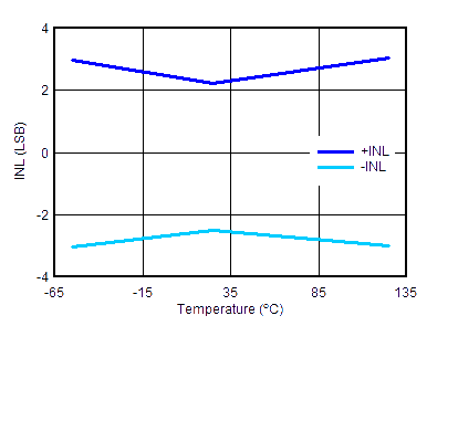 Figure 6-12 Minimum and Maximum INL vs Temperature
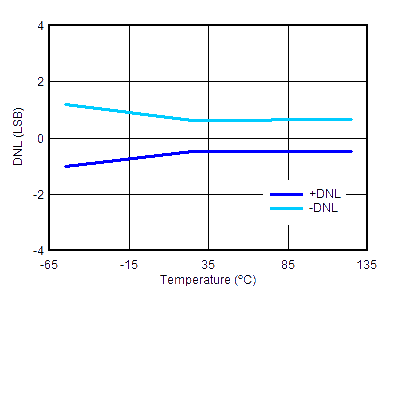 Figure 6-14 Minimum and Maximum DNL vs Temperature
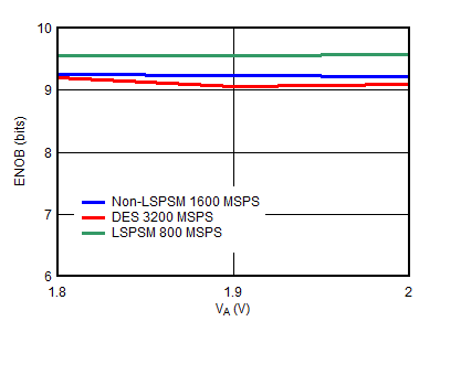 Figure 6-16 ENOB vs Supply Voltage
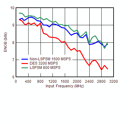 Figure 6-18 ENOB vs Input Frequency
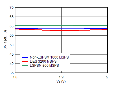 Figure 6-20 SNR vs Supply Voltage
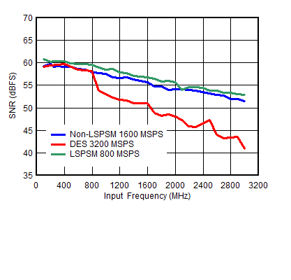 Figure 6-22 SNR vs Input Frequency
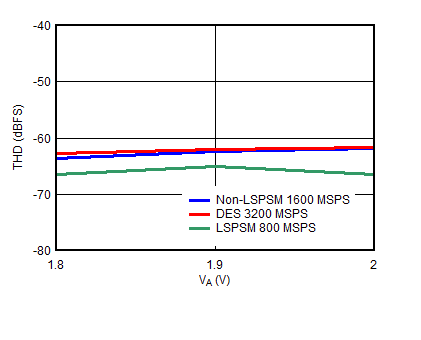 Figure 6-24 THD vs Supply Voltage
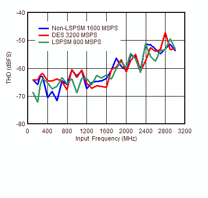 Figure 6-26 THD vs Input Frequency
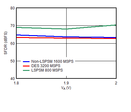 Figure 6-28 SFDR vs Supply Voltage
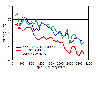 Figure 6-30 SFDR vs Input Frequency
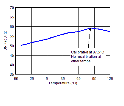
| fCLK = 1.6 GHz | fIN = 248 MHz |
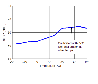
| fCLK = 1.6 GHz | fIN = 248 MHz |
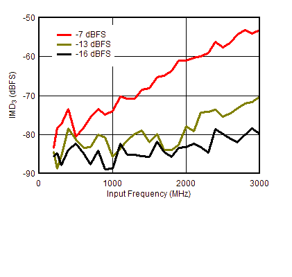 Figure 6-36 3rd Order Intermodulation Distortion vs Input Frequency (DES Mode 3200 MSPS)
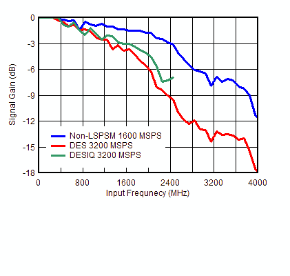 Figure 6-38 Insertion Loss vs Input Frequency