JAJSDJ8A April 2017 – October 2021 ADC12D1620QML-SP
PRODUCTION DATA
- 1 特長
- 2 アプリケーション
- 3 概要
- 4 Revision History
- 5 Pin Configuration and Functions
-
6 Specifications
- 6.1 Absolute Maximum Ratings
- 6.2 ESD Ratings
- 6.3 Recommended Operating Conditions
- 6.4 Thermal Information
- 6.5 Converter Electrical Characteristics: Static Converter Characteristics
- 6.6 Converter Electrical Characteristics: Dynamic Converter Characteristics
- 6.7 Converter Electrical Characteristics: Analog Input/Output and Reference Characteristics
- 6.8 Converter Electrical Characteristic: Channel-to-Channel Characteristics
- 6.9 Converter Electrical Characteristics: LVDS CLK Input Characteristics
- 6.10 Electrical Characteristics: AutoSync Feature
- 6.11 Converter Electrical Characteristics: Digital Control and Output Pin Characteristics
- 6.12 Converter Electrical Characteristics: Power Supply Characteristics
- 6.13 Converter Electrical Characteristics: AC Electrical Characteristics
- 6.14 Electrical Characteristics: Delta Parameters
- 6.15 Timing Requirements: Serial Port Interface
- 6.16 Timing Requirements: Calibration
- 6.17 Quality Conformance Inspection
- 6.18 Timing Diagrams
- 6.19 Typical Characteristics
-
7 Detailed Description
- 7.1 Overview
- 7.2 Functional Block Diagram
- 7.3 Feature Description
- 7.4 Device Functional Modes
- 7.5
Programming
- 7.5.1
Control Modes
- 7.5.1.1
Non-ECM
- 7.5.1.1.1 Dual-Edge Sampling Pin (DES)
- 7.5.1.1.2 Non-Demultiplexed Mode Pin (NDM)
- 7.5.1.1.3 Dual Data-Rate Phase Pin (DDRPh)
- 7.5.1.1.4 Calibration Pin (CAL)
- 7.5.1.1.5 Low-Sampling Power-Saving Mode Pin (LSPSM)
- 7.5.1.1.6 Power-Down I-Channel Pin (PDI)
- 7.5.1.1.7 Power-Down Q-Channel Pin (PDQ)
- 7.5.1.1.8 Test-Pattern Mode Pin (TPM)
- 7.5.1.1.9 Full-Scale Input-Range Pin (FSR)
- 7.5.1.1.10 AC- or DC-Coupled Mode Pin (VCMO)
- 7.5.1.1.11 LVDS Output Common-Mode Pin (VBG)
- 7.5.1.2 Extended Control Mode
- 7.5.1.1
Non-ECM
- 7.5.1
Control Modes
- 7.6 Register Maps
- 8 Application Information Disclaimer
- 9 Power Supply Recommendations
- 10Layout
- 11Device and Documentation Support
- 12Mechanical, Packaging, and Orderable Information
パッケージ・オプション
デバイスごとのパッケージ図は、PDF版データシートをご参照ください。
メカニカル・データ(パッケージ|ピン)
- FVA|256
- NAA|376
サーマルパッド・メカニカル・データ
発注情報
8.1.1.2 Driving the ADC in DES Mode
The ADC12D1620 can be configured as either a 2-channel, 1.6 GSPS device (Non-DES mode) or a 1-channel 3.2-GSPS device (DES mode). When the device is configured in DES mode, there is a choice for with which input to drive the single-channel ADC. These are the 3 options:
DES – externally driving the I-channel input only. This is the default selection when the ADC is configured in DES mode. It may also be referred to as DESI for added clarity.
DESQ – externally driving the Q-channel input only.
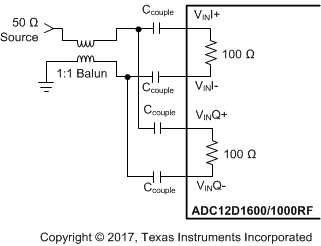
DESIQ, DESCLKIQ – externally driving both the I- and Q-channel inputs. VinI+ and VinQ+ must be driven with the exact same signal. VinI- and VinQ- must be driven with the exact same signal, which is the differential complement to the one driving VinI+ and VinQ+.
The input impedance for each I and Q input is 100-Ω differential (or 50-Ω single-ended), so the trace to each VinI+, VinI-, VinQ+, and VinQ- must always be 50-Ω single-ended. If a single I or Q input is being driven, then that input presents a 100-Ω differential load. For example, if a 50-Ω single-ended source is driving the ADC, a 1:2 balun transforms the impedance to 100-Ω differential. However, if the ADC is being driven in DESIQ mode, then the 100-Ω differential impedance from the I input appears in parallel with the Q input for a composite load of 50-Ω differential, and a 1:1 balun would be appropriate. See Figure 8-1 for an example circuit driving the ADC in DESIQ mode. A recommended part selection uses the mini-circuits TC1-1-13MA+ balun with Ccouple = 0.22 µF.
 Figure 8-1 Driving DESIQ Mode
when only one channel is used in non-DES mode or the ADC is driven in DESI or DESQ mode, terminate the unused analog input to reduce any noise coupling into the ADC. See Table 8-1 for details.
| MODE | POWER DOWN | COUPLING | RECOMMENDED TERMINATION |
|---|---|---|---|
| Non-DES | Yes | AC-DC | Tie Unused+ and Unused– to VBG |
| DES/Non-DES | No | DC | Tie Unused+ and Unused– to VBG |
| DES/Non-DES | No | AC | Tie Unused+ to Unused– |