JAJSF36L November 2008 – February 2019 ADC14155QML-SP
PRODUCTION DATA.
- 1 特長
- 2 アプリケーション
- 3 概要
- 4 改訂履歴
- 5 Pin Configuration and Functions
-
6 Specifications
- 6.1 Absolute Maximum Ratings
- 6.2 ESD Ratings
- 6.3 Recommended Operating Conditions
- 6.4 Thermal Information
- 6.5 ADC14155 Converter Electrical Characteristics DC Parameters
- 6.6 ADC14155 Converter Electrical Characteristics (Continued) DYNAMIC Parameters
- 6.7 ADC14155 Converter Electrical Characteristics (Continued) Logic and Power Supply Electrical Characteristics
- 6.8 ADC14155 Converter Electrical Characteristics (Continued) Timing and AC Characteristics
- 6.9 Timing Diagram
- 6.10 Transfer Characteristic
- 6.11 Typical Performance Characteristics, DNL, INL
- 6.12 Typical Performance Characteristics, Dynamic Performance
- 7 Detailed Description
- 8 Application and Implementation
- 9 Power Supply Recommendations
- 10Layout
- 11デバイスおよびドキュメントのサポート
- 12メカニカル、パッケージ、および注文情報
パッケージ・オプション
デバイスごとのパッケージ図は、PDF版データシートをご参照ください。
メカニカル・データ(パッケージ|ピン)
- NBA|48
サーマルパッド・メカニカル・データ
発注情報
8.1 Application Information
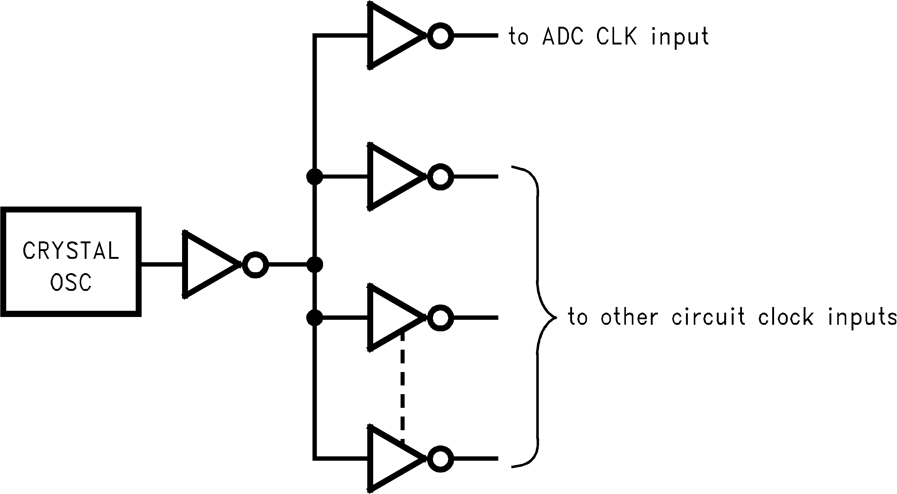
To achieve the best dynamic performance, the clock source driving the CLK input must have a sharp transition region and be free of jitter. Isolate the ADC clock from any digital circuitry with buffers, as with the clock tree shown in Figure 23. The gates used in the clock tree must be capable of operating at frequencies much higher than those used if added jitter is to be prevented. Best performance will be obtained with a differential clock input drive, compared with a single-ended drive.
As mentioned in Power Supply Recommendations, it is good practice to keep the ADC clock line as short as possible and to keep it well away from any other signals. Other signals can introduce jitter into the clock signal, which can lead to reduced SNR performance, and the clock can introduce noise into other lines. Even lines with 90° crossings have capacitive coupling, so try to avoid even these 90° crossings of the clock line.
 Figure 23. Isolating the ADC Clock From Other Circuitry With a Clock Tree